Manufacturing method of split-gate flash memory

A manufacturing method and technology of flash memory, which is applied to semiconductor devices, electrical components, circuits, etc., can solve problems affecting the basic performance of devices, inter-channel punch-through, etc., and achieve the effect of improving punch-through performance and performance

Active Publication Date: 2021-04-13
SHANGHAI HUALI MICROELECTRONICS CORP
View PDF3 Cites 0 Cited by
  • Summary
  • Abstract
  • Description
  • Claims
  • Application Information

AI Technical Summary

Problems solved by technology

The realization of the basic performance of Silvo Flash often requires the coordination and cooperation between different gates, which is easy to produce the punch-through phenomenon between the channels, which greatly affects the basic performance of the device

Method used


Image

  • Manufacturing method of split-gate flash memory
  • Manufacturing method of split-gate flash memory
  • Manufacturing method of split-gate flash memory

Examples


Embodiment Construction

[0046] The manufacturing method of the existing split-gate flash memory:

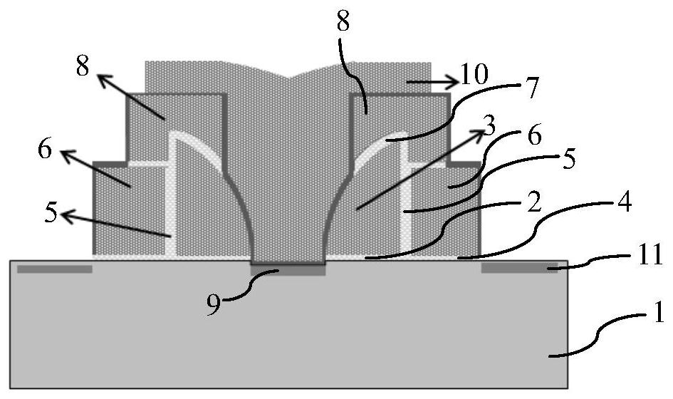
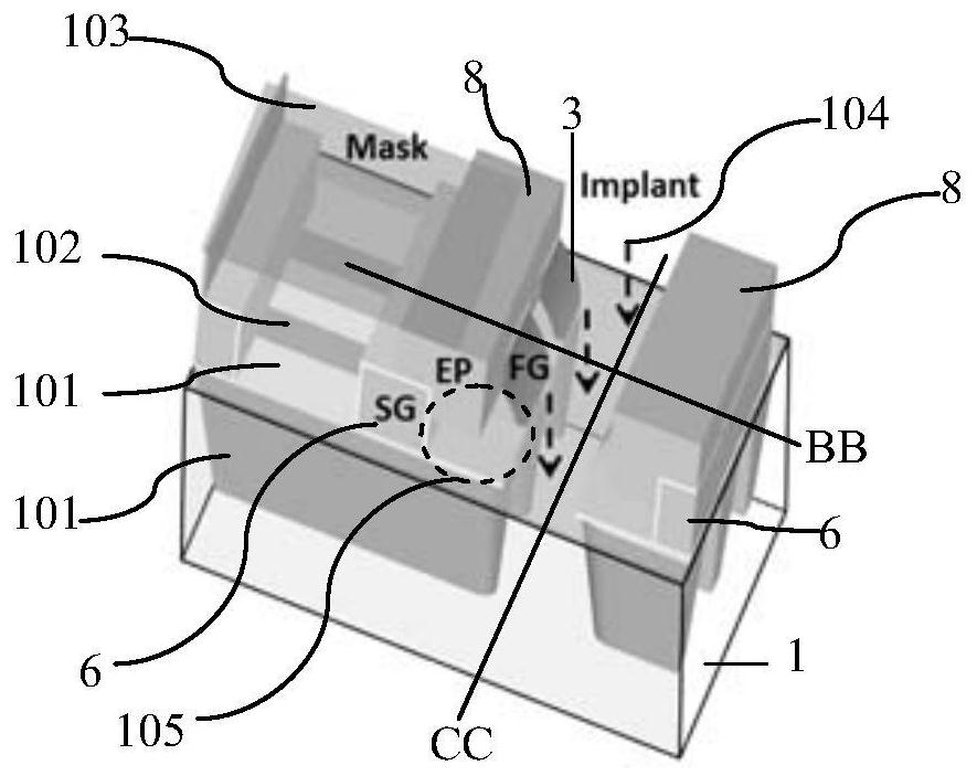
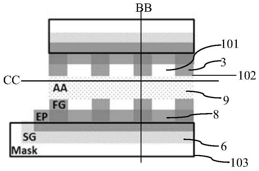
[0047] Because the method of the embodiment of the present invention is obtained by further analyzing the technical problems existing in the existing method, so before introducing the existing method in detail, introduce the existing method, such as figure 1 Shown is a schematic diagram of the cell structure of the split-gate flash memory formed by the existing method; as Figure 2A As shown, it is a perspective view of the device in the source injection of the existing manufacturing method of split-gate flash memory; as Figure 2B Shown is the top view of the device in the source injection of the existing split-gate flash memory manufacturing method. For the cell structure of the split-gate flash memory formed by the existing method, please refer to figure 1 As shown, the manufacturing method of the existing split-gate flash memory includes the following steps:

[0048] Step 1, such as figure 1As sh...


PUM


Abstract

The invention discloses a method for manufacturing a split-gate flash memory, comprising: forming field oxygen in a semiconductor substrate and isolating a plurality of active regions, each active region comprising a plurality of active regions in a stripe structure and parallel to each other Rows, the rows of active regions corresponding to the source regions are connected to form a whole line in the column direction and form active region columns; select gates are formed, and each select gate is in a strip-shaped column structure and parallel to each other; floating gates are formed, and the floating gates are formed in On the row of the active region on the first side of the corresponding selection gate; forming an erasing gate, each erasing gate covers the top surface of the first side of the selection gate and extends to the top of the floating gate; Covering the vertical sides of the region column with a dielectric layer; forming a photoresist pattern to open the active region column, part of the erasing gate near the first side, and each floating gate outside the first side; performing source injection. The invention can protect the floating gate during the source injection, prevent the source injection from affecting channel penetration, thereby improving the performance of the device.

Description

technical field [0001] The invention relates to a method for manufacturing a semiconductor integrated circuit, in particular to a method for manufacturing a split-gate flash memory (Flash). Background technique [0002] With the development of the times, Flash, as a low-cost, easy-to-program and erase non-volatile memory, has been more and more widely used. Recently, Super (Super) Flash based on split gate or split gate technology has received widespread attention. Compared with conventional Flash, the structure of split gate Flash is more complicated, with a special structure of multi-layer polysilicon (Ploy), For example, the ESF3 Flash of Silicon Storage Technology (SST). Compared with the traditional Flash, this novel split-gate Flash has the advantages of excellent reliability and no over-erasing due to the use of a thicker tunnel dielectric layer. At present, the typical SST ESF3 has shown remarkable application prospects in the fields of automotive electronics, micr...

Claims


Application Information

Patent Timeline
Patent Type & Authority Patents(China)
IPC IPC(8): H01L27/11524
Inventor 王小川张磊胡涛王奇伟陈昊瑜
Owner SHANGHAI HUALI MICROELECTRONICS CORP
Why Eureka
Try Eureka