Photodiode and forming method thereof, image sensor and fingerprint imaging module

A photodiode and bottom electrode technology, applied in circuits, electrical components, semiconductor devices, etc., can solve the problems of small lighting area of ​​image sensors and affect the quality of fingerprint images.

Inactive Publication Date: 2019-05-07
SHANGHAI OXI TECH
View PDF3 Cites 4 Cited by
  • Summary
  • Abstract
  • Description
  • Claims
  • Application Information

AI Technical Summary

Problems solved by technology

[0004] However, the image sensor used in the existing fingerprint imaging module has a small lighting area, which affects the quality of the obtained fingerprint image.

Method used


Image

  • Photodiode and forming method thereof, image sensor and fingerprint imaging module
  • Photodiode and forming method thereof, image sensor and fingerprint imaging module
  • Photodiode and forming method thereof, image sensor and fingerprint imaging module

Examples


Embodiment Construction

[0051]It can be seen from the background art that the image sensor used in the optical fingerprint imaging module in the prior art has insufficient light-gathering area, resulting in the problem of poor quality of fingerprint images obtained.

[0052] The image sensor used in the fingerprint imaging module usually includes a pixel array, and the pixel array includes a plurality of pixel units arranged in an array, and the pixel units include photodiodes, and the photodiodes are used to collect fingerprints carrying fingerprint information. light to obtain fingerprint images.

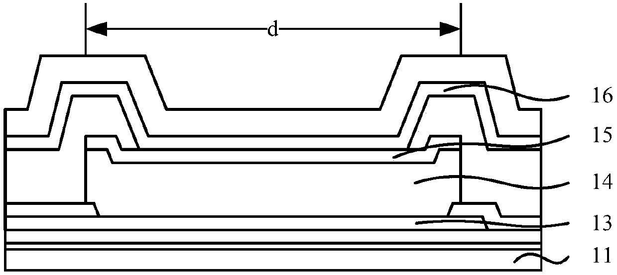
[0053] refer to figure 1 , shows a schematic cross-sectional structure diagram of a photodiode in an image sensor used in a fingerprint imaging module.

[0054] The photodiode includes: a substrate 11; a first dielectric layer 12, the first dielectric layer 12 is located on the substrate 11; a bottom electrode 13, the bottom electrode 13 is located on the first dielectric layer 12; A photosensitive lay...


PUM


Abstract

A photodiode and a forming method thereof, an image sensor and a fingerprint imaging module are provided. The forming method of the photodiode includes the following steps: providing a substrate; forming a bottom electrode on the substrate; forming a photosensitive layer on the bottom electrode; and processing the photosensitive layer by laser to form an uneven surface of the photosensitive layer.After the formation of the photosensitive layer, the photosensitive layer is processed by laser to form an uneven surface, so as to increase the surface area of the photosensitive layer, reduce the surface reflection loss of the photosensitive layer and achieve the purpose of improving the light collection ability of the formed photodiode and improving the image quality without increasing the size of the opening.

Description

technical field [0001] The invention relates to the field of fingerprint imaging, in particular to a photodiode and its forming method, an image sensor, and a fingerprint imaging module. Background technique [0002] Fingerprint recognition is to compare the fingerprint image with the existing fingerprint information in the fingerprint recognition system after collecting the human fingerprint image to realize identity recognition. Due to the convenience of use and the uniqueness of human fingerprints, fingerprint recognition technology has been widely used in various fields, such as: public security bureaus, customs and other security inspection fields, building access control systems, and consumer products such as personal computers and mobile phones, etc. [0003] Among the fingerprint imaging technologies used in fingerprint identification, one is to collect human fingerprint images through optical methods: incident light is generated by a light source; the incident light...

Claims


Application Information

Patent Timeline
Patent Type & Authority Applications(China)
IPC IPC(8): H01L31/0352H01L31/18
Inventor 曲志刚朱虹
Owner SHANGHAI OXI TECH
Why Eureka
Try Eureka