Analog signal test circuit

An analog signal and analog testing technology, applied in analog circuit testing, electronic circuit testing, etc., can solve the problems of difficult direct observation, low amplification ability, low testing efficiency, etc., and achieve the effect of eliminating mutual interference.

Inactive Publication Date: 2019-05-10
HUADA SEMICON CO LTD
View PDF7 Cites 0 Cited by
  • Summary
  • Abstract
  • Description
  • Claims
  • Application Information

AI Technical Summary

Problems solved by technology

[0005] (1) There are mutual influences between the various analog modules, for example, the current may pass through the switch circuit, which will cause noise problems in the analog test, affect the test accuracy, and the test efficiency is low; and
[0006] (2) Since the driving ability of key test nodes is generally weak, if the test node directly outputs, the amplification ability is low, which directly makes it difficult to directly observe. Therefore, it is generally necessary to attach a buffer to each test node to amplify the test node. analog nodes, which results in higher circuit cost and larger circuit area

Method used


Image

  • Analog signal test circuit
  • Analog signal test circuit
  • Analog signal test circuit

Examples


Embodiment Construction

[0032] It should be noted that components in the various figures may be shown exaggerated for the purpose of illustration and are not necessarily true to scale. In the various figures, identical or functionally identical components are assigned the same reference symbols.

[0033] In the present invention, unless otherwise specified, "arranged on", "arranged on" and "arranged on" do not exclude the presence of intermediates between the two.

[0034] In the present invention, each embodiment is only intended to illustrate the solutions of the present invention, and should not be construed as limiting.

[0035] In the present invention, unless otherwise specified, the quantifiers "a" and "an" do not exclude the scene of multiple elements.

[0036] It should also be pointed out here that in the embodiments of the present invention, for the sake of clarity and simplicity, only a part of parts or components may be shown, but those skilled in the art can understand that under the t...


PUM


Abstract

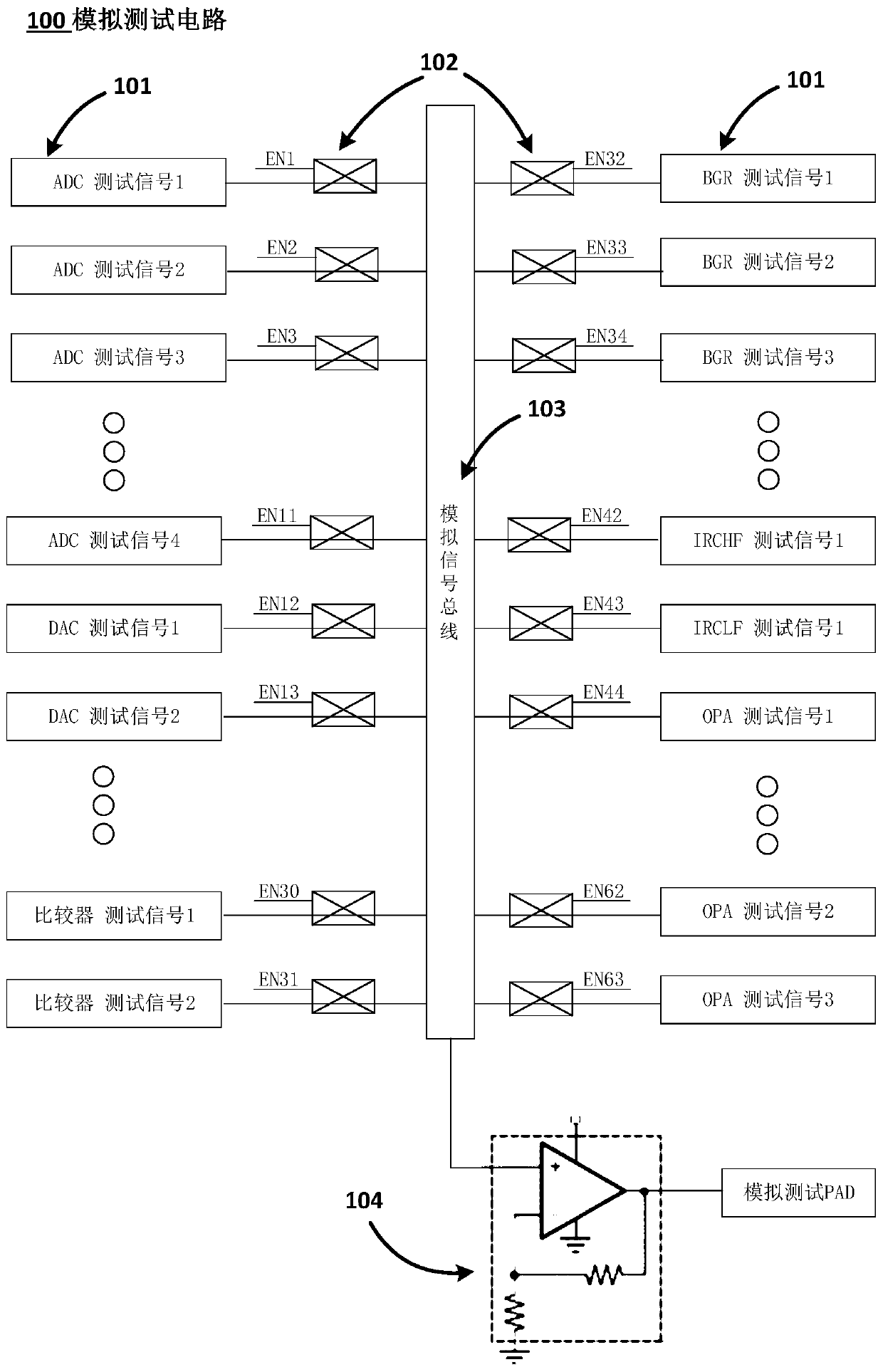
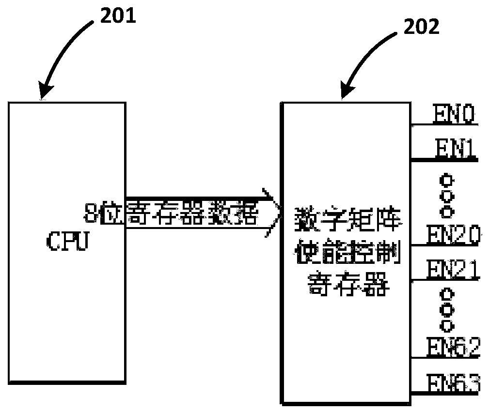
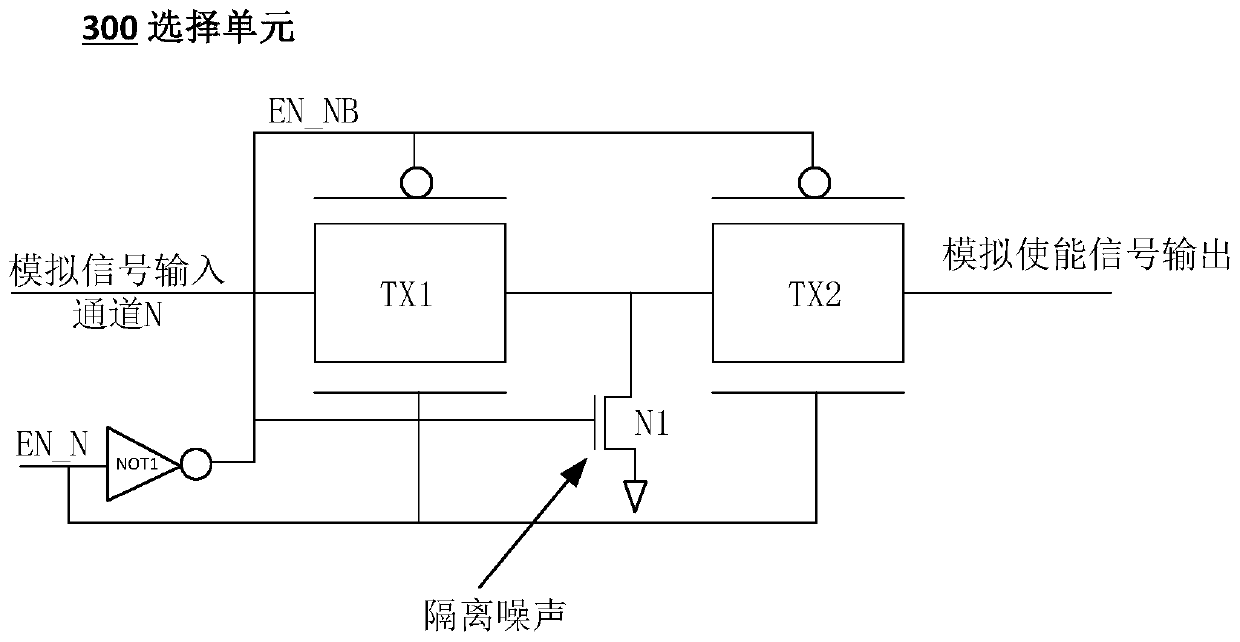
The present invention relates to an analog signal test circuit. The analog signal test circuit comprises: a plurality of analog signal input channels configured to receive an analog test signal; a channel gating circuit having an input end connected with the analog signal input channels and having an output end connected with an analog signal bus, wherein the channel gating circuit is configured to selectively connect or disconnect with the analog signal input channels; the analog signal bus connected with the channel gating circuit and connected with a buffer, wherein the analog signal bus isconfigured to transmit the selectively connected analog test signal to the buffer; and a buffer circuit having an input end connected with the analog signal bus and having an output end being the output end of the analog test signal, wherein the buffer circuit is configured to perform buffer and output on the analog test signal transmitted by the analog signal bus. The analog signal test circuitcan reduce the mutual interference between test nodes, can reduce the number of buffers and can ensure the high drive capability.

Description

technical field [0001] The present invention generally relates to the field of circuit testing, and specifically relates to an analog signal testing circuit. Background technique [0002] Electronic devices such as Micro Control Unit (MCU) and Embedded System (SOC) need to carry out their analog circuits and digital circuits respectively in the design stage, such as chip test (ChipProbing) and final test (Final Test) stage, and / or manufacturing stage. Tests to verify the functionality of individual modules or components. [0003] For digital circuit testing, the test circuit for MCU includes, for example, a scan chain, and the test circuit for internal memory includes, for example, BIST (Built-in Self Test). [0004] For the analog circuit test, there is no relatively complete test circuit or test method at present. The main test method currently used is to directly input the analog signal excitation, and then measure the output analog signal. However, such a testing appr...

Claims


Application Information

Patent Timeline
Patent Type & Authority Applications(China)
IPC IPC(8): G01R31/316
Inventor 刘慧谢文录
Owner HUADA SEMICON CO LTD
Why Eureka
Try Eureka