3D NAND storage and forming method thereof

A 3DNAND and memory technology, which is applied in the manufacture of electric solid-state devices, semiconductor devices, and semiconductor/solid-state devices, etc. It can solve the problems of poor sidewall morphology of gate separation grooves, and achieve the effect of improving the performance of the common source of the array.

Active Publication Date: 2019-05-10
YANGTZE MEMORY TECH CO LTD
View PDF6 Cites 7 Cited by
  • Summary
  • Abstract
  • Description
  • Claims
  • Application Information

AI Technical Summary

Problems solved by technology

[0004] In order to further increase the storage capacity, the prior art usually forms a multi-layer stack structure when forming the stack structure, and each layer stack structure includes several alternately stacked isolation layers and sacrificial layers, and the stacking of adjacent layers A thick silicon oxide layer is formed between the structures, and by etching the multilayer stacked structure and the thick silicon oxide layer between the stacked structures, a gate spacer that exposes the surface of the substrate is formed, but the sidewall of the gate spacer poor shape

Method used


Image

  • 3D NAND storage and forming method thereof
  • 3D NAND storage and forming method thereof
  • 3D NAND storage and forming method thereof

Examples


Embodiment 3

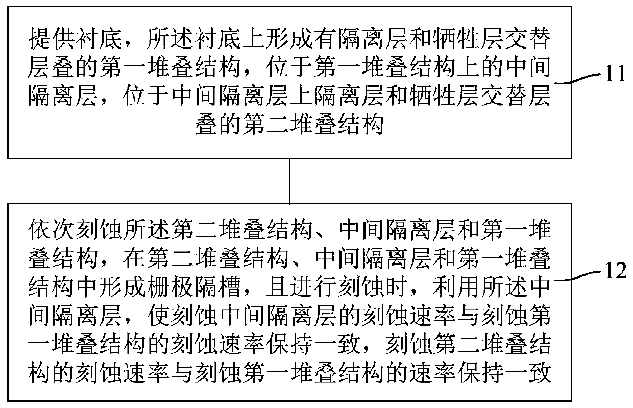
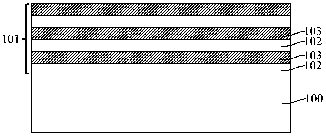
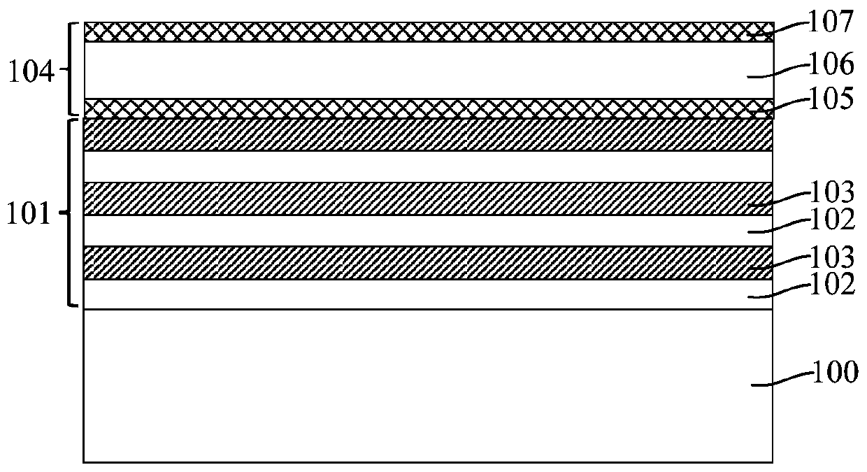
[0090] Figure 11-13 It is a schematic cross-sectional structure diagram of the formation process of the gate spacer of the 3D NAND memory according to another embodiment of the present invention. The difference between this embodiment and the foregoing embodiments lies in the specific structure of the isolation layer and the manner in which the etching rate for etching the intermediate isolation layer is consistent with the etching rate for etching the first stack structure and the second stack structure. It should be noted that, for descriptions or limitations of the same or similar structures in this embodiment as in the foregoing embodiments, please refer to the descriptions or limitations of corresponding parts in the foregoing embodiments, and details are not repeated in this embodiment.

[0091] In one embodiment, please refer to Figure 11 and Figure 12 , during etching, the method for keeping the etching rate of the intermediate isolation layer consistent with the ...


PUM


Abstract

The invention discloses a 3D NAND storage and a forming method thereof. The forming method of the 3D NAND storage has the steps of forming an intermediate isolation layer between a first stacking structure and a second stacking structure; and sequentially etching the second stacking structure, the intermediate isolation layer and the first stacking structure, wherein when grid partition slots arein the second stacking structure, the middle isolation layer and the first stacking structure, by using the intermediate isolation layer, the etching speed for etching the intermediate isolation layeris consistent with that for etching the first stacking structure, and the etching speed for etching the second stacking structure is consistent with that for etching the first stacking structure, sothat the bending defect of the side wall of the grid partition slots caused when the speed for etching the intermediate insulating layer is different from the etching speeds for etching the first stacking structure and the second stacking structure can be avoided.

Description

technical field [0001] The invention relates to the field of semiconductor manufacturing, in particular to a 3D NAND memory and a forming method thereof. Background technique [0002] NAND flash memory is a better storage device than hard disk drives, and it has been widely used in electronic products as people pursue non-volatile storage products with low power consumption, light weight and high performance. At present, the NAND flash memory with a planar structure is close to the limit of practical expansion. In order to further increase the storage capacity and reduce the storage cost per bit, a 3D NAND memory with a 3D structure is proposed. [0003] The manufacturing process of the existing 3D NAND memory includes: providing a substrate on which a stacked structure in which isolation layers and sacrificial layers are alternately stacked; etching the stacked structure to form an exposed substrate surface in the stacked structure channel hole; form a storage structure in...

Claims


Application Information

Patent Timeline
Patent Type & Authority Applications(China)
IPC IPC(8): H01L21/66H01L21/67H01L27/1157H01L27/11578
Inventor 袁野任连娟刘青松程强
Owner YANGTZE MEMORY TECH CO LTD
Why Eureka
Try Eureka