Semiconductor device and preparation method thereof

A semiconductor and device technology, which is applied in the field of semiconductor devices and their preparation, can solve the problems that the SiP growth thickness cannot meet the contact requirements, the contact process cannot be turned on, and breaks through, so as to meet the subsequent contact process requirements, improve thickness, and enhance growth. Effect

Pending Publication Date: 2022-04-12
SHANGHAI INTEGRATED CIRCUIT EQUIP & MATERIALS IND INNOVATION CENT CO +1
View PDF0 Cites 0 Cited by
  • Summary
  • Abstract
  • Description
  • Claims
  • Application Information

AI Technical Summary

Problems solved by technology

[0004] However, the existing SiP (silicon phosphide) growth technology for FinFET devices relies on direct growth after etching trenches.
With the scaling of technology nodes, the SiP growth in the long channel region is limited due to the reduction in the size of the SiP in the short channel region and the reduction in the size between the long channel lines, resulting in the thickness of the SiP growth at the bottom of the trench in the long channel region. The contact requirements cannot be met, resulting in the problem that the contact process cannot turn on the S / D (source / drain) or break through the S / D

Method used


Image

  • Semiconductor device and preparation method thereof
  • Semiconductor device and preparation method thereof
  • Semiconductor device and preparation method thereof

Examples


Embodiment Construction

[0030] The semiconductor device and its manufacturing method proposed by the present invention will be further described in detail below with reference to the accompanying drawings and specific embodiments. The advantages and features of the present invention will be more apparent from the following description. It should be noted that all the drawings are in a very simplified form and use imprecise scales, and are only used to facilitate and clearly assist the purpose of illustrating the embodiments of the present invention.

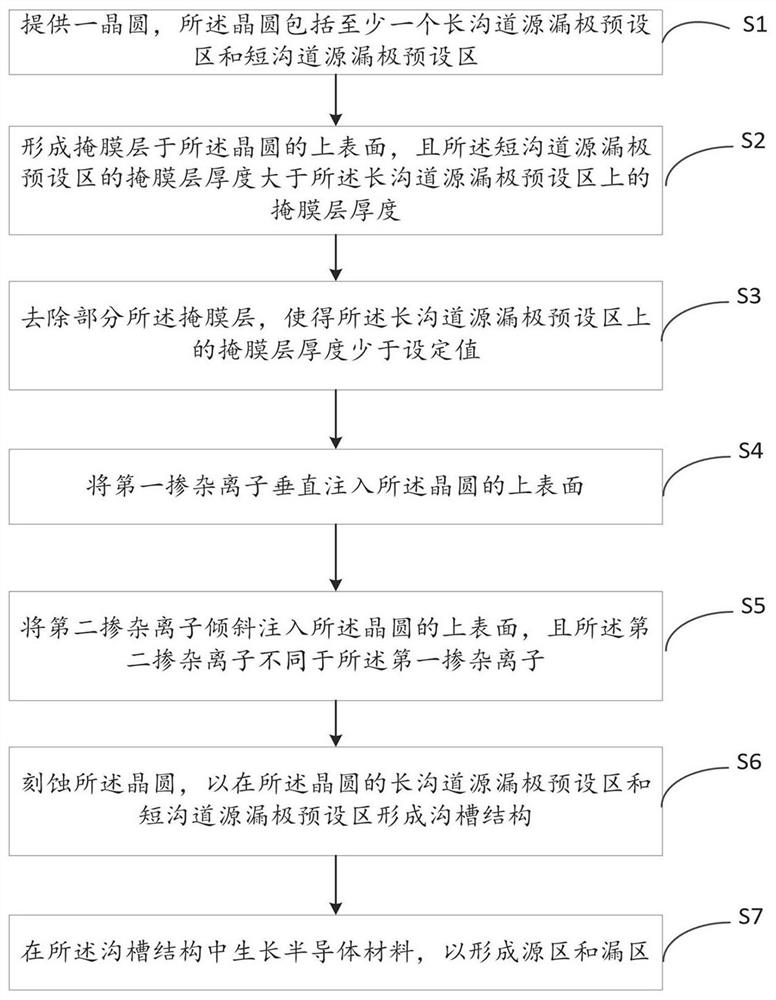
[0031] Please refer to figure 1 , the invention provides a method for preparing a semiconductor device, comprising the following steps:

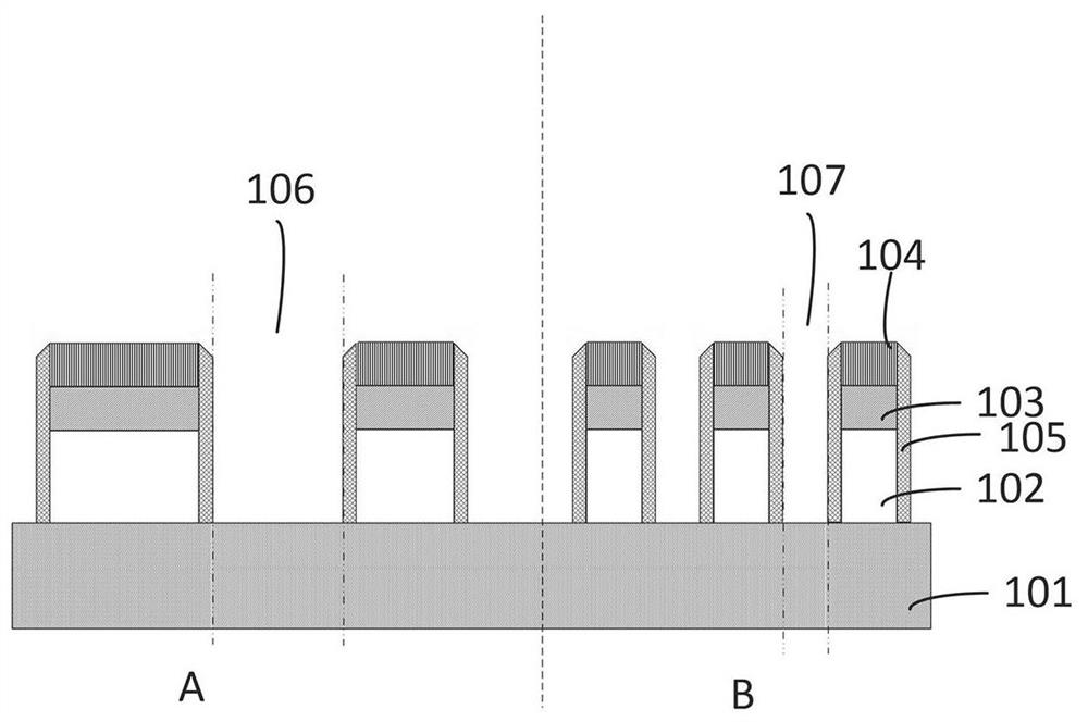
[0032] Step S1: providing a wafer, the wafer includes at least one long-channel source-drain preset region and a short-channel source-drain preset region;

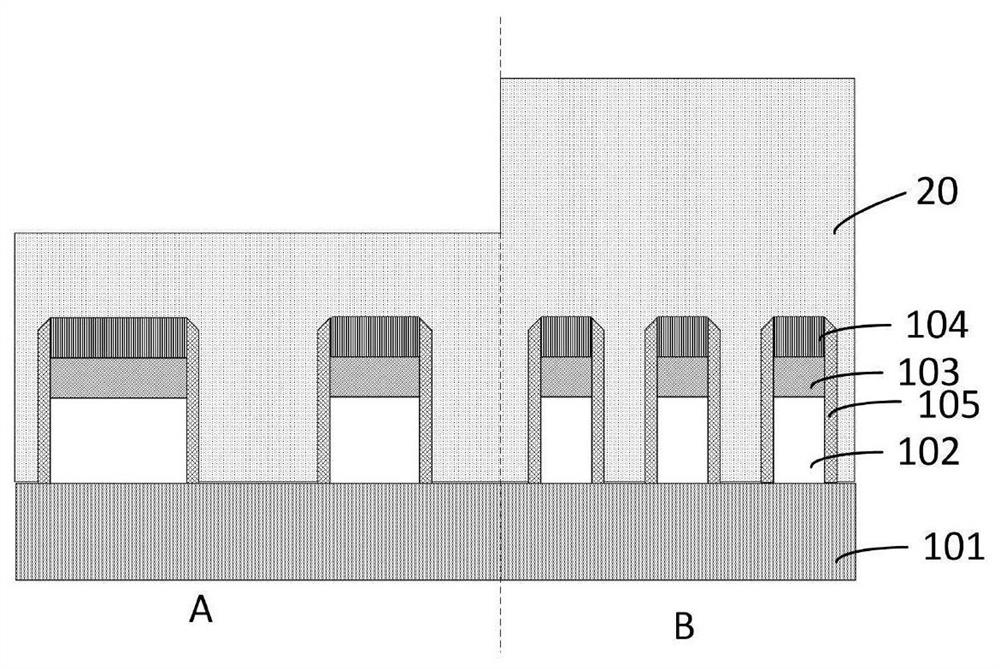
[0033] Step S2: forming a mask layer on the upper surface of the wafer, and the thickness of the mask layer on the short-channel source-drain preset region is g...


PUM


Abstract

The invention provides a semiconductor device and a preparation method thereof, and the preparation method of the semiconductor device comprises the following steps: providing a wafer which comprises at least one long-channel source drain electrode preset region and at least one short-channel source drain electrode preset region; forming a mask layer on the upper surface of the wafer, wherein the thickness of the mask layer on the short channel source drain electrode preset region is greater than that of the mask layer on the long channel source drain electrode preset region; part of the mask layer is removed, so that the thickness of the mask layer on the long-channel source-drain electrode preset region is smaller than a set value; implanting first doping ions into the upper surface of the wafer; second doping ions are injected into the upper surface of the wafer; etching the wafer to form groove structures in the long channel source and drain electrode preset region and the short channel source and drain electrode preset region of the wafer; and growing a semiconductor material in the trench structure to form a source region and a drain region. According to the preparation method of the semiconductor device, the growth thickness of the semiconductor material in the long channel region can be improved.

Description

technical field [0001] The invention relates to the technical field of integrated circuits, in particular to a semiconductor device and a preparation method thereof. Background technique [0002] The semiconductor integrated circuit (IC) industry has undergone rapid development. During the development of ICs, functional density, the number of interconnected devices per chip area, has generally increased, while geometry size, the smallest device or interconnect that can be made using a fabrication process, has decreased. The improvement of IC performance is mainly achieved by continuously shrinking the size of integrated circuit devices to increase its speed. The advantages of this scaled-down process are increased production efficiency and reduced associated costs. At the same time, this scaled-down process also increases the complexity of handling and manufacturing ICs. [0003] In the process of seeking higher device density, higher performance and lower cost, as the in...

Claims


Application Information

Patent Timeline
IPC IPC(8): H01L21/266H01L29/08
Inventor 卢越野刘轶群
Owner SHANGHAI INTEGRATED CIRCUIT EQUIP & MATERIALS IND INNOVATION CENT CO
Why Eureka
Try Eureka