Test structure for testing etching process, forming method thereof, and testing method

A technology for testing structures and testing methods, which is applied in the fields of technology for producing decorative surface effects, microstructure technology, microstructure devices, etc., and can solve the problems of inability to truly and reliably reflect the influence of etching processes, low accuracy, and test results. Poor reliability and other problems, to achieve the effect of simple and fast testing, reliability and accuracy improvement

Active Publication Date: 2017-02-22
SEMICON MFG INT (SHANGHAI) CORP
View PDF5 Cites 0 Cited by
  • Summary
  • Abstract
  • Description
  • Claims
  • Application Information

AI Technical Summary

Problems solved by technology

[0005] However, when using test equipment to test the two-dimensional test structure, the test results obtained have poor reliability and low accuracy, which cannot truly and reliably reflect the impact of the etching process on the MEMS device

Method used


Image

  • Test structure for testing etching process, forming method thereof, and testing method
  • Test structure for testing etching process, forming method thereof, and testing method
  • Test structure for testing etching process, forming method thereof, and testing method

Examples


Embodiment Construction

[0040] It can be seen from the background art that the testing method provided by the prior art has poor reliability and low accuracy, and cannot truly and reliably reflect the influence of the etching process on the MEMS device.

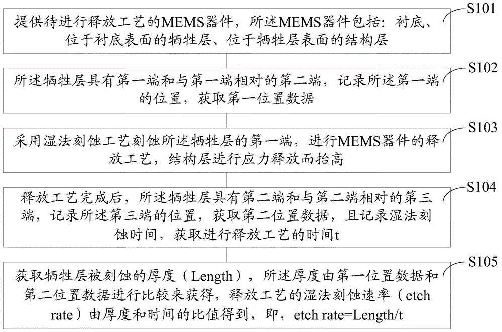
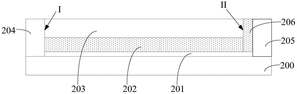
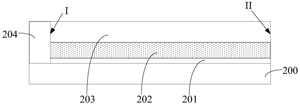
[0041] Please refer to figure 1 , figure 1 It is a schematic flow chart of a test method: step S101, providing a MEMS device to be released, and the MEMS device includes: a substrate, a sacrificial layer on the surface of the substrate, and a structural layer on the surface of the sacrificial layer; step S102, the The sacrificial layer has a first end and a second end opposite to the first end, the position of the first end is recorded, and the first position data is obtained; step S103, etching the second end of the sacrificial layer by a wet etching process At one end, the release process of the MEMS device is performed, and the structural layer is lifted by stress release; step S104, after the release process is completed, the sacrificial layer ...


PUM


Abstract

The invention provides a test structure used for testing etching process and a formation method and a testing method thereof. The test structure comprises a substrate, a structure layer and a first plug, wherein the substrate is provided with a first sacrificial layer on the surface, the structure layer is arranged on the surface of the first sacrificial layer and is provided with a first end and a second end opposite to the first end, the crystal constant of the structure layer is different from that of the first sacrificial layer, the surface of the structure layer contacting with the first sacrificial layer is provided with stress, the first plug is arranged at the first end of the structure layer and penetrates the structure layer and the first sacrificial layer to be arranged on the surface of the substrate, and the material of the first plug is different from that of the first sacrificial layer. By the test structure, testing is simple and quick, the test structure is directly linked to MEMS (micro-electromechanical systems) device, and reliability and accuracy in testing are improved.

Description

technical field [0001] The invention relates to the technology in the field of semiconductor manufacturing, in particular to a test structure for testing an etching process, a forming method and a testing method thereof. Background technique [0002] Micro-Electro-Mechanical System (MEMS for short) mainly includes micro-mechanisms, micro-sensors, micro-actuators and corresponding processing circuits. High-tech cutting-edge disciplines developed on the basis of achievements. The development of MEMS technology has opened up a new technical field and industry. Micro sensors, micro actuators, micro components, micro mechanical optical devices, vacuum microelectronic devices, power electronic devices, etc. made by MEMS technology are widely used in aviation, aerospace, automobile, There are very broad application prospects in biomedicine, environmental monitoring, military affairs and almost all fields that people come into contact with. [0003] The release process is a key li...

Claims


Application Information

Patent Timeline
Patent Type & Authority Patents(China)
IPC IPC(8): B81B7/00B81C1/00
Inventor 郑超郭亮良王伟
Owner SEMICON MFG INT (SHANGHAI) CORP
Why Eureka
Try Eureka