Manufacturing process of copper-coin-buried board

A technology for burying copper blocks and making methods, which is applied in the manufacture of printed circuits, electrical components, and the removal of conductive materials by chemical/electrolytic methods, can solve problems such as reducing defect rates, reduce production difficulty, save costs, and solve problems Effects of poorly exposed quality issues

Active Publication Date: 2019-05-17
KINWONG ELECTRONICS TECH LONGCHUAN
View PDF5 Cites 2 Cited by
  • Summary
  • Abstract
  • Description
  • Claims
  • Application Information

AI Technical Summary

Problems solved by technology

[0005] The technical problem to be solved by the present invention is how to improve the flatness of the board, avoid warping of the board during the laser conformask process, and reduce the defective rate

Method used


Image

  • Manufacturing process of copper-coin-buried board

Examples


Embodiment Construction

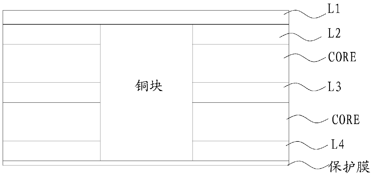
[0018] The technical solutions in the embodiments of the present invention will be clearly and completely described below in conjunction with the drawings in the embodiments of the present invention, and similar component numbers in the drawings represent similar components. Apparently, the embodiments described below are only a part of the embodiments of the present invention, rather than all the embodiments. Based on the embodiments of the present invention, all other embodiments obtained by persons of ordinary skill in the art without creative efforts fall within the protection scope of the present invention.

[0019] It should be understood that when used in this specification and the appended claims, the terms "comprising" and "comprises" indicate the presence of described features, integers, steps, operations, elements and / or components, but do not exclude one or Presence or addition of multiple other features, integers, steps, operations, elements, components and / or col...


PUM


Abstract

The invention discloses a manufacturing process of a copper-coin-buried PCB, and relates to the technical field of PCB board manufacture. The method comprises the following steps: laminating->millingan edge->drilling an alignment hole->conformask of an outer circuit->etching an inner layer->AOI of the inner layer->tearing off a protective film->removing excessive glue->laser drilling. In the laminating step, the protective film is at the lowermost layer of the PCB. The invention completes the step of removing excessive glue which affects board warpage after the conformask of the outer circuit, effectively avoids the problem of warpage during the circuit manufacture, reduces the production difficulty, solves the quality problem of poor exposure of the original conventional process, and improves the product yield.

Description

technical field [0001] The invention relates to the technical field of circuit manufacturing of PCBs, in particular to a manufacturing process of a buried copper block board. Background technique [0002] The circuit production of conventional PCB boards is to paste a layer of photosensitive material on the PCB substrate, and use the UV light emitted by the exposure lamp in the exposure machine to trigger the reaction of the photosensitive initiator in the photosensitive material to achieve selective partial bridge polymerization. Hardening effect, so as to achieve the purpose of graphic transfer. [0003] At present, there are two types of exposure machines in the PCB industry, one is a conventional vacuum-type manual or CCD automatic exposure machine, and the other is a non-vacuum type laser direct imaging LDI exposure machine. The difference between the two is: the former needs to use negative film as a tool for graphic transfer, the tool will expand with heat and contra...

Claims


Application Information

Patent Timeline
Patent Type & Authority Applications(China)
IPC IPC(8): H05K3/00H05K3/06
Inventor 张柏勇张鸿伟蓝春华姚承林
Owner KINWONG ELECTRONICS TECH LONGCHUAN
Why Eureka
Try Eureka