Manufacturing method of display panel and photomask of display panel

A technology for a display panel and a manufacturing method, which is applied to the photolithographic process of the pattern surface, the photolithographic process exposure device, semiconductor/solid-state device manufacturing, etc., and can solve the problem of large channel region width, small on-state current, and active switching performance. Missing and other problems, to achieve the effect of increasing the etching depth

Active Publication Date: 2019-05-21
HKC CORP LTD
View PDF5 Cites 0 Cited by
  • Summary
  • Abstract
  • Description
  • Claims
  • Application Information

AI Technical Summary

Problems solved by technology

Half-exposure can be realized by half-tone mask (HTM, Half Tone Mask). However, since the formation of the active switch requires two steps of dry etching and two steps of wet etching, the active switch formed by this method has a channel The width of the area is large, which is not conducive to the development of subsequent manufacturing processes, and will cause the on-state current (Ion) of the TFT to be small, which may easily cause problems such as insufficient charging of the display panel, loss of active switching performance, or leakage.

Method used


Image

  • Manufacturing method of display panel and photomask of display panel
  • Manufacturing method of display panel and photomask of display panel
  • Manufacturing method of display panel and photomask of display panel

Examples


Embodiment Construction

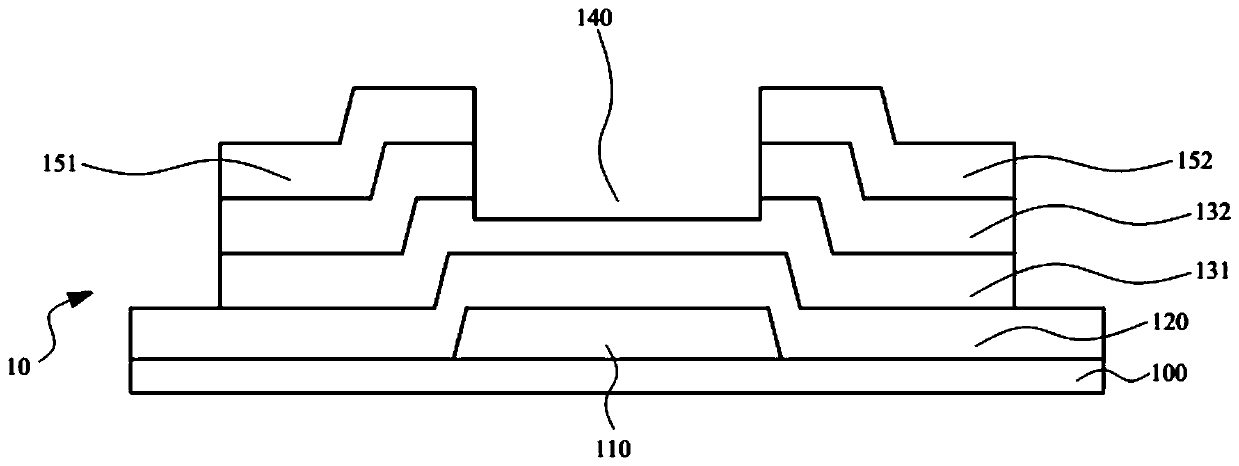
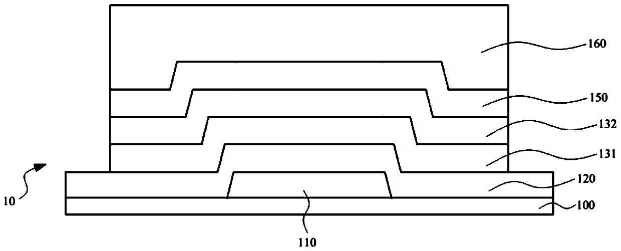
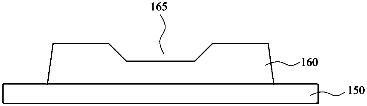
[0028] The following descriptions of the various embodiments refer to the attached drawings to illustrate specific embodiments that the present application can be implemented in. The directional terms mentioned in this application, such as "up", "down", "front", "rear", "left", "right", "inside", "outside", "side", etc., are for reference only The orientation of the attached schema. Therefore, the directional terms used are used to illustrate and understand the application, but not to limit the application.

[0029] The drawings and descriptions are to be regarded as illustrative in nature and not restrictive. In the figures, structurally similar units are denoted by the same reference numerals. In addition, the size and thickness of each component shown in the drawings are arbitrarily shown for understanding and convenience of description, but the present application is not limited thereto.

[0030] In the drawings, the thickness of layers, films, panels, regions, etc., ar...


PUM

PropertyMeasurementUnit
widthaaaaaaaaaa
widthaaaaaaaaaa
widthaaaaaaaaaa

Abstract

The invention provides a manufacturing method of a display panel and a photomask of the display panel. The manufacturing method comprises the steps of: providing a first substrate; setting a grid layer on the first substrate; setting a grid insulation layer on the first substrate and the grid layer; setting a source layer and a drain layer on the grid insulation layer; and forming a channel regionbetween the source layer and the drain layer through the photomask, wherein the photomask is provided with a channel region pattern which is provided with a light supplementing pattern on the sourcelayer or the drain layer, and through the light supplementing pattern, the light of the photomask can reach the channel region.

Description

technical field [0001] The present application relates to the field of display, in particular to a method for manufacturing a display panel and a photomask thereof. Background technique [0002] TFT-LCD (Thin Film Transistor Liquid Crystal Display, thin film transistor liquid crystal display device), has the advantages of low cost, low power consumption and high performance, and is widely used in the fields of electronics and digital products. important display platform. The driving of the pixel unit in the TFT-LCD needs to be realized by driving the corresponding scanning lines and data lines through the gate driving circuit and the source driving circuit. With the increasing demand for panel size, resolution, and image quality with large viewing angles, as well as further improving user experience and saving costs, various manufacturers have developed many manufacturing technologies related to the display field. [0003] Compared with the five mask (5Mask) process, the f...

Claims


Application Information

Patent Timeline
Patent Type & Authority Applications(China)
IPC IPC(8): H01L21/77H01L27/12G03F1/76G03F7/20
Inventor 张合静卓恩宗
Owner HKC CORP LTD
Why Eureka
Try Eureka