
Quantum confined stark effect electroabsorption modulator on a soi platform

A technology of electroabsorption modulator and multiple quantum wells, which is applied in the fields of instruments, nanotechnology, optical waveguide and light guide, etc., and can solve the problem of 2V driving voltage of difficult CMOS driver

Active Publication Date: 2019-05-21
ROCKLEY PHOTONICS INC
View PDF4 Cites 0 Cited by
  • Summary
  • Abstract
  • Description
  • Claims
  • Application Information

AI Technical Summary

Problems solved by technology

Due to the limitations of germanium material properties (band gap and absorption), the problems that make SiGe QCSE EAM operate at O ​​band on 3 μm SOI platform include 1) SiGe multi-quantum well epitaxy (EPI) stack that can operate at 1.3 μm wavelength Design; 2) Design of the coupling structure that brings light from a 3 μm SOI waveguide into a low lossy SiGe multiple quantum well (MQW) waveguide; and 3) difficulty in achieving 2V drive voltage with CMOS drivers due to carrier barrier effect in the MQW region

Method used


Image

  • Quantum confined stark effect electroabsorption modulator on a soi platform
  • Quantum confined stark effect electroabsorption modulator on a soi platform
  • Quantum confined stark effect electroabsorption modulator on a soi platform

Examples


Embodiment Construction

[0049] The detailed description set forth below in connection with the accompanying drawings is intended as a description of exemplary embodiments of electroabsorption modulators provided in accordance with the present invention and is not intended to represent the only forms in which the invention may be constructed or utilized. This description sets forth the features of the invention in conjunction with the illustrated embodiments. It should be understood, however, that the same or equivalent functions and structures can be achieved by different embodiments, which are also intended to be within the spirit and scope of the present invention. As indicated elsewhere herein, like element numbers are intended to refer to like elements or features.

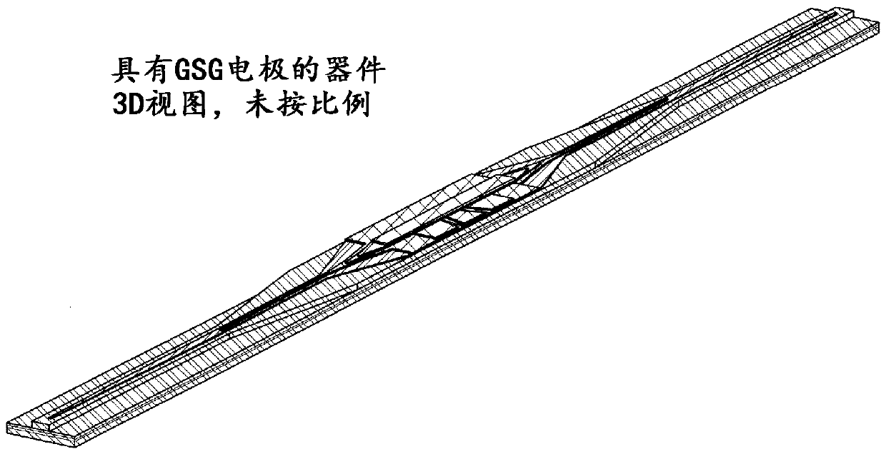
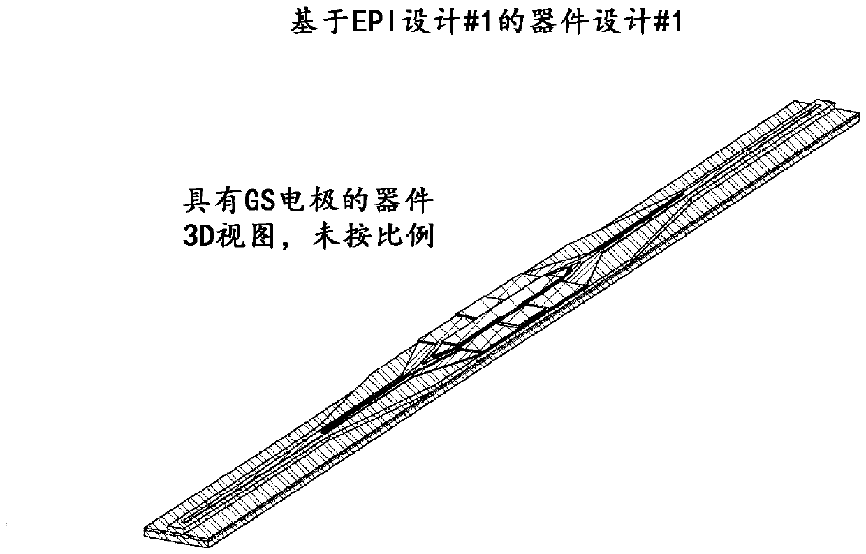
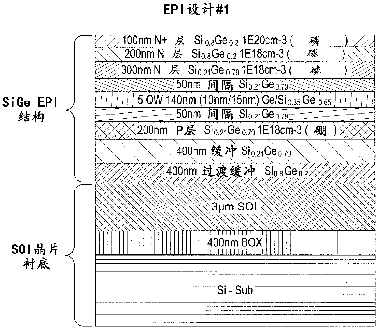
[0050] The first embodiment ("EPI Design #1") is shown in Figure 1 to Figure 9 middle.

[0051] figure 1 An example of a SiGe EPI structure according to the invention is shown, where a thin layer of transition buffer SiGe is inse...


PUM

PropertyMeasurementUnit
Thicknessaaaaaaaaaa
Thicknessaaaaaaaaaa
Thicknessaaaaaaaaaa

Abstract

The invention provides a electroabsorption modulator. The modulator comprises an SOI waveguide; an active region, the active region comprising amultiple quantum well (MQW) region; and a coupler for coupling the SOI waveguide to the active region. The coupler comprising: a transit waveguide coupling region;a buffer waveguide coupling region; and a taper region; wherein, the transit waveguide coupling region couples light between the SOI waveguide and the buffer waveguide coupling region; and the buffer waveguide coupling region couples light between the transit waveguide region and the active region via the taper region.

Description

technical field [0001] The present invention relates to modulators and to optical coupling within modulators on SOI platforms, and more particularly to SiGe Quantum Confined Stark Effect (QCSE) modulators. Background technique [0002] It is expected to fabricate high-speed SiGe quantum-confined Stark-effect (QCSE) electroabsorption modulators (EAMs) operating at the O-band (1.3 μm wavelength) and compatible CMOS on SOI platforms for data center networking applications. Due to the limitations of germanium material properties (band gap and absorption), the problems that make SiGe QCSE EAM operate at O ​​band on 3 μm SOI platform include 1) SiGe multi-quantum well epitaxy (EPI) stack that can operate at 1.3 μm wavelength Design; 2) Design of the coupling structure that brings light from a 3 μm SOI waveguide into a low Lossy SiGe multiple quantum well (MQW) waveguides; and 3) Difficulty in achieving 2V drive voltage with CMOS drivers due to carrier barrier effect in the MQW re...

Claims


Application Information

Patent Timeline
IPC IPC(8): G02F1/017
CPCG02F1/01708G02F1/01716G02B6/12004G02B6/1228G02F1/01725G02B6/14G02F1/0157B82Y20/00
Inventor 余国民
Owner ROCKLEY PHOTONICS INC
Learn More