Bias circuit of electroabsorption modulated laser

An electro-absorption modulator and electro-absorption modulation technology, applied in laser parts, differential amplifiers, DC-coupled DC amplifiers, etc., can solve the problem of large negative voltage ripple, unstable electro-absorption modulation laser bias circuit, and easy Problems such as external interference

Active Publication Date: 2012-07-11
SHENZHEN NEOPHOTONICS TECH
View PDF5 Cites 17 Cited by
  • Summary
  • Abstract
  • Description
  • Claims
  • Application Information

AI Technical Summary

Problems solved by technology

However, the negative voltage ripple output by this method is relatively large, which is easily affected b...

Method used


Image

  • Bias circuit of electroabsorption modulated laser
  • Bias circuit of electroabsorption modulated laser
  • Bias circuit of electroabsorption modulated laser

Examples


Embodiment Construction

[0013] The preferred embodiment of the present invention will be described in detail below in conjunction with the accompanying drawings.

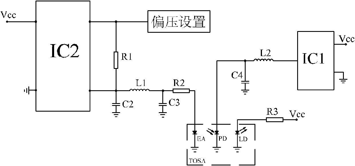
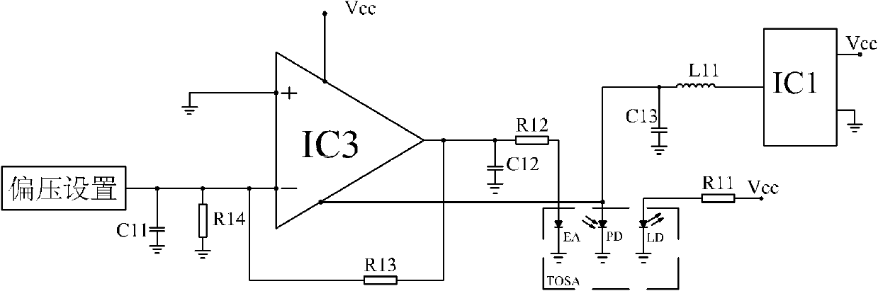
[0014] like figure 2 The shown bias circuit for an electroabsorption modulated laser includes: a TOSA (Transmitter Optical Sub-Assembly) composed of an electroabsorption modulator EA, a semiconductor laser LD and a monitor diode PD with a common cathode grounded , the anode of the semiconductor laser LD is connected to the power supply Vcc (value 3V or 5V) through the first current limiting resistor R11. A switching charge pump or switching tube chip IC1 with a non-adjustable output voltage, its positive power supply pin is connected to the power supply Vcc, its negative power supply pin is grounded, its output pin is connected to one end of the first inductor L11, and the other end of the inductor L11 is connected to the anode of the monitoring diode PD and the first One end of the third filtering capacitor C13, and the other end of...


PUM


Abstract

The invention provides a bias circuit of an electroabsorption modulated circuit. The bias circuit comprises a light emitting assembly TOSA (Transmitter Optical Sub Assembly), a conversion charge pump with nonadjustable output voltage or a switch tube chip, an operation amplifier, and a feedback resistor, wherein the light emitting assembly TOSA is composed of an electroabsorption modulator EA, a semiconductor laser LD and a monitor diode PD, which have a common grounded cathode; the anode of the semiconductor laser LD is connected with a power supply Vcc through a first current limiting resistor; the conversion charge pump or the switch tube chip has a positive power pin connected with the power supply Vcc, a grounded negative power pin, and an output pin connected with one end of a first inductor; the other end of the inductor is connected with the anode of the monitor diode PD and with one end of a third filter capacitor; the other end of the capacitor is grounded; the operation amplifier has a positive power pin connected with the power supply Vcc, a negative power pin connected with the anode of the monitor diode PD, a grounded positive input pin, a negative input pin connected with an external bias unit through a loop resistor, and an output pin connected with the anode of the electroabsorption modulator EA; and the feedback resistor is connected between the negative input pin and the output pin of the operation amplifier.

Description

technical field [0001] The invention relates to an externally adjusted laser bias circuit, in particular to an electric absorption modulated laser bias circuit. Background technique [0002] In order to realize the transmission of data on the optical fiber, the signal needs to undergo electro-optical conversion and photoelectric conversion through the optical fiber transceiver, and the electro-optical conversion is completed by the semiconductor laser. According to different modulation methods, semiconductor lasers are mainly divided into two types: direct modulation lasers and external modulation lasers. In medium and long-distance transmission, externally modulated lasers are mainly used. Although this type of laser has a complex structure and high cost, it can obtain a large dispersion tolerance value, and the transmission distance is mostly more than 40 kilometers. Externally modulated lasers include: electroabsorption modulated lasers and lithium niobate modulated las...

Claims


Application Information

Patent Timeline
IPC IPC(8): H03F3/45H01S3/02
Inventor 任礼霞夏京盛
Owner SHENZHEN NEOPHOTONICS TECH
Why Eureka
Try Eureka