Peripheral coupled traveling wave electro-absorption modulator

a modulator and traveling wave technology, applied in the field of optoelectronics, can solve the problems of limiting the saturation optical power of the modulator typically to a few milliwatts, and not taking full advantage of traveling wave interactions

Inactive Publication Date: 2007-01-23
RGT UNIV OF CALIFORNIA
View PDF5 Cites 17 Cited by
  • Summary
  • Abstract
  • Description
  • Claims
  • Application Information

AI Technical Summary

Problems solved by technology

At such short interaction lengths, they do not take full advantage of traveling wave interactions.
The high density of the optical field in the EA layer of an EA modulator of such a small mode also limits the saturation optical power of the modulator typically to a few milliwatts.

Method used


Image

  • Peripheral coupled traveling wave electro-absorption modulator
  • Peripheral coupled traveling wave electro-absorption modulator
  • Peripheral coupled traveling wave electro-absorption modulator

Examples


Embodiment Construction

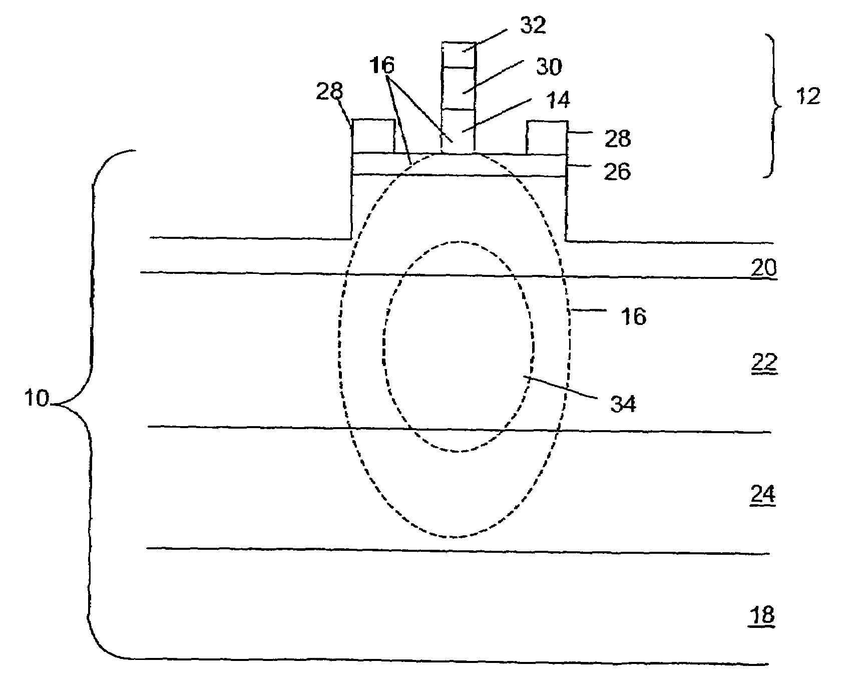
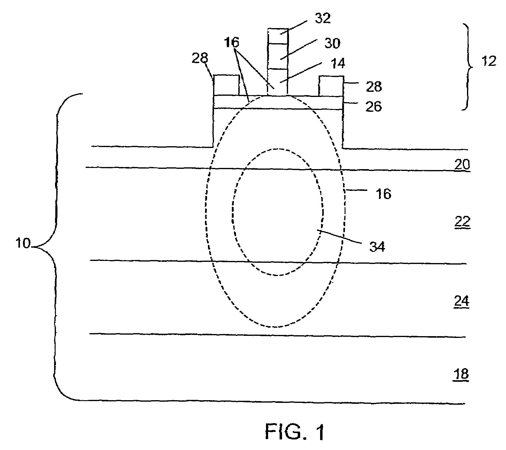
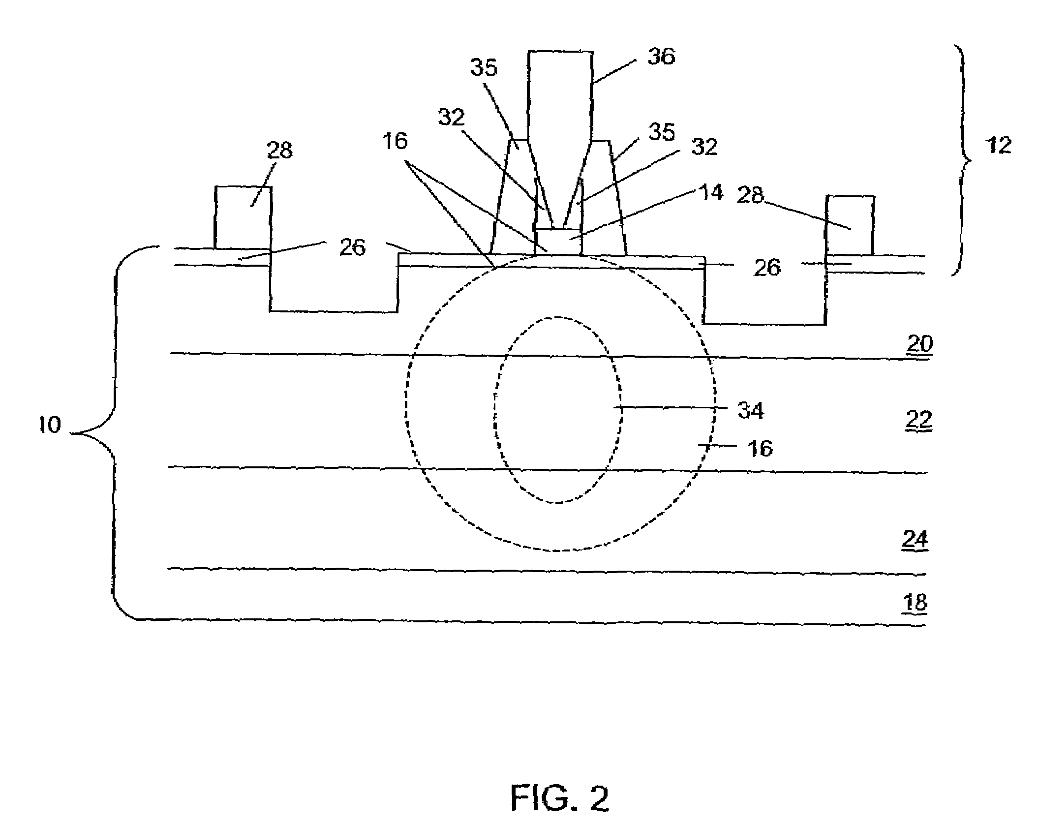
[0009]Broadly stated, embodiments of the invention use peripheral coupling of a microwave wave and an optical wave. With the invention, strong EA modulation may be achieved. Embodiments of the invention may achieve number of benefits, including separation of design optimization for optical waveguides and microwave waveguides working together to modulate an optical wave; provision of a millimeters-long synchronized length for interaction between a microwave wave and an optical wave obtaining a very low modulation voltage; microwave transmission line design with low attenuation and impedance matching to the source; relatively easy optical coupling to fibers; and large optical saturation power compared to other EA modulators.

[0010]Turning now to FIG. 1, showing a schematic cross-section of an embodiment of the invention, an apparatus for optical modulation includes an optical waveguide 10 and a microwave waveguide 12. Microwave waveguide 12 has an EA material 14 sized and placed such t...


PUM

PropertyMeasurementUnit
optical saturation poweraaaaaaaaaa
thicknessaaaaaaaaaa
widthaaaaaaaaaa

Abstract

A method for optical modulation comprising the steps of guiding an optical wave in an optical waveguide, the optical wave having an evanescent tail; and applying a modulation voltage to the evanescent tail.

Description

PRIORITY CLAIM[0001]Applicants claim priority benefits under 35 U.S.C. § 119 on the basis of patent application No. 60 / 392,073, filed Jun. 28, 2002.TECHNICAL FIELD[0002]The invention is in the optoelectronic field. The invention is applicable to optical modulation systems.BACKGROUND ART[0003]Optical modulators are used in a variety of applications. Controlled modulation of light is useful in analog systems to produce an output proportional to the input signal. Digital optical systems, such as fiber optic communication systems, use optical modulators to impose digital signals on light. Digital optical modulators as signaling devices may also form the basis for optical memories and general computer devices.[0004]One form of optical modulation is electro-absorption (hereinafter, “EA”) modulation. In conventional EA modulation, EA material is an integral part of the optical waveguide. Consequently, the design of the microwave waveguide is constrained by the optical waveguide design. It ...

Claims


Application Information

Patent Timeline
Patent Type & Authority Patents(United States)
IPC IPC(8): G02F1/17F28F1/12G02F1/017
CPCB82Y20/00G02F1/01708G02F2201/127G02F2201/063
Inventor CHANG, WILLIAM S. C.YU, PAUL K. L.
Owner RGT UNIV OF CALIFORNIA
Why Eureka
Try Eureka