Semiconductor photonoic nano communication link method

a technology of photonoic nano and semiconductor, applied in the direction of instruments, optical elements, optical waveguide light guides, etc., can solve the problems of unsatisfactory material set for lasing, modulation, detection functions, etc., to improve photonic modulation, absorption and gain functions, and relax phonon-assistance rule effects

Inactive Publication Date: 2011-03-15
AIR FORCE US SEC THE THE
View PDF12 Cites 17 Cited by
  • Summary
  • Abstract
  • Description
  • Claims
  • Application Information

AI Technical Summary

Benefits of technology

[0014]It is another object of the invention to provide a combination of Silicon, Germanium and Tin materials usable for improved photonic modulation, absorption and gain func

Problems solved by technology

Achieving chip-to-chip and intra-chip photonic interconnects in Silicon on insulator (SOI) complementary metal oxide semiconductor (CMOS) and in BiCMOS presents an extreme challenge to active photonic devices because the energy used in the optical communication link of such devices i

Method used


Image

  • Semiconductor photonoic nano communication link method
  • Semiconductor photonoic nano communication link method
  • Semiconductor photonoic nano communication link method

Examples


Embodiment Construction

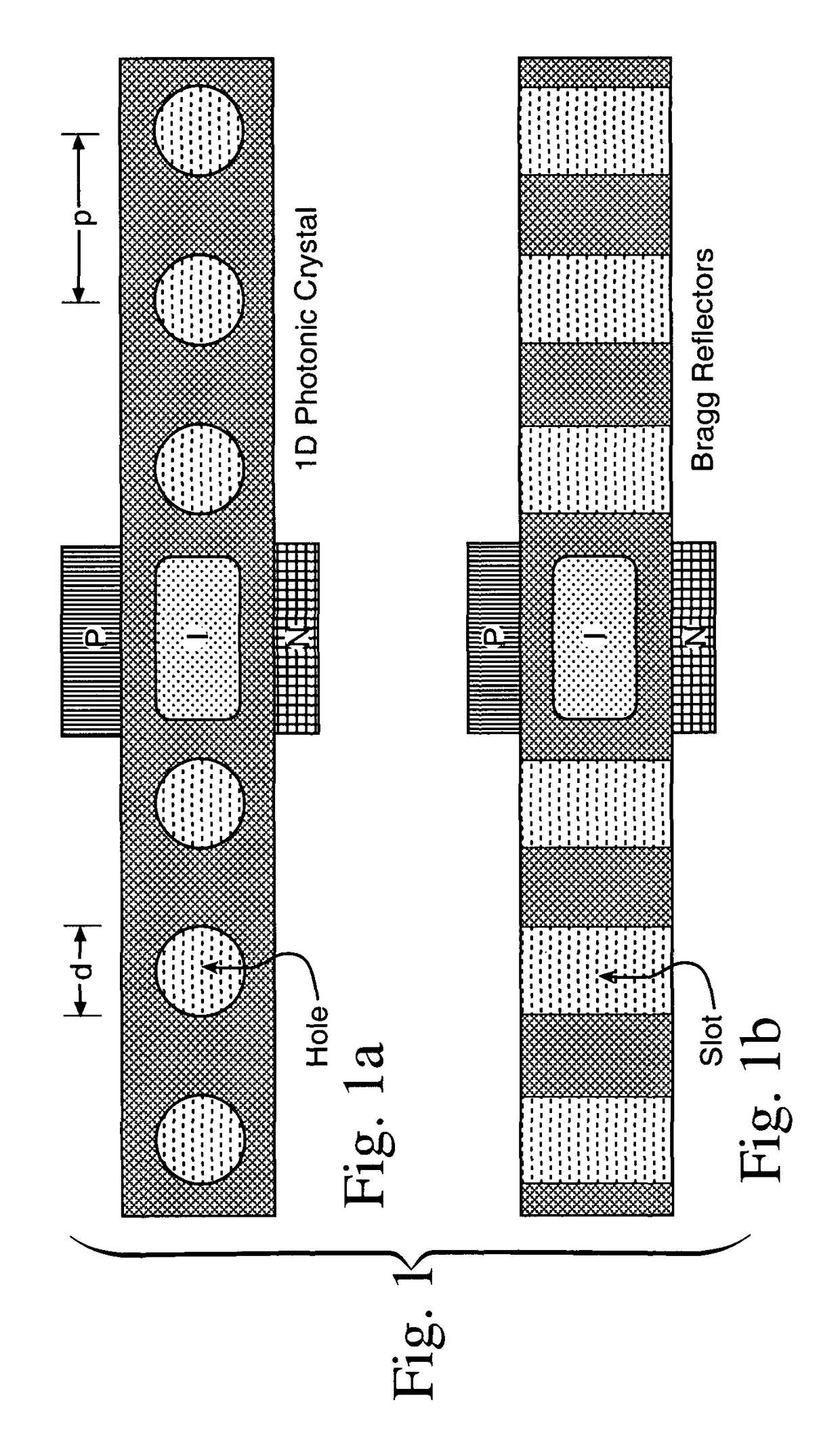
[0033]In this invention, the basic structure for each photonic communication link device is a Silicon-on-insulator strip waveguide (i.e., a Silicon nanowire) that becomes a rib waveguide locally along a resonator length, such a waveguide is shown in the views of the FIG. 1 drawing. This FIG. 1 waveguide contains a one-dimensional photonic-crystal (PhC) structure providing a spaced pair of PhC reflectors defining an active micro cavity. Reflectors may be a set of air or oxide filled holes etched through the Silicon strip, or a set of deeply etched air or oxide filled slots that define Bragg-grating mirrors straddling the cavity. Typically, these holes and slots are filled with Silicon dioxide, SiO2. The resonator is located in the hole-defect(s) or slot-defect(s) of the 1D lattice as shown in FIGS. 1a and 1b, respectively. The local rib regions do not disturb significantly the propagating mode in the SOI strip

[0034]For the 1550 nanometer wavelength spectral region, the hole diameter,...


PUM


Abstract

An optical signal low energy method for coupling electrical signals on-chip between component circuits of for example a CMOS circuit array. The described coupling method employs infrared signals communicated along a nano-scale resonant semiconductor waveguide between for example PIN diode signal transducers. The coupling may employ an electrically pumped laser, an electro absorption modulator and a photodetector all for typically the 1.5 to 2.0 micrometer spectral region with each formed using for example PIN heterodiode semiconductor devices. Each of these three devices includes active semiconductor crystal material situated in a resonator within a strip waveguide. The resonator is defined by two fabricated mirrors having a tapered location one dimensional photonic crystal lattice of oxide hole or slot apertures. Each semiconductor device is for example a heterodiode pumped or controlled by laterally disposed wings enclosing the resonator to form a lateral PIN structure for current injection or high E-field generation. CMOS compatible ten gigabit per second signals of low energy use per transmitted bit are achieved.

Description

RIGHTS OF THE GOVERNMENT[0001]The invention described herein may be manufactured and used by or for the Government of the United States for all governmental purposes without the payment of any royalty.BACKGROUND OF THE INVENTION[0002]Achieving chip-to-chip and intra-chip photonic interconnects in Silicon on insulator (SOI) complementary metal oxide semiconductor (CMOS) and in BiCMOS presents an extreme challenge to active photonic devices because the energy used in the optical communication link of such devices is desirably less than 100 femto Joules (10−15 Joules) per data bit transmitted. This is the energy dissipated by the coupled photonic link comprised of a continuous wave laser, a fast modulator and a photodetector. As devices become optimized, this energy should be “down-scalable” year-by-year. This link constraint, may also be expressed in terms of milliwatts per Gigabit of communicated data and is a key to making photonic interconnects superior to copper interconnects. A s...

Claims


Application Information

Patent Timeline
IPC IPC(8): H04B10/00
CPCH04B10/25H04B10/801
Inventor SOREF, RICHARD A.
Owner AIR FORCE US SEC THE THE
Why Eureka
Try Eureka