Crystal epitaxial structure and growth method
An epitaxial growth and epitaxial structure technology, applied in semiconductor devices, photovoltaic power generation, sustainable manufacturing/processing, etc., to achieve the effects of reducing strain, reducing thickness, and suppressing dislocations
- Summary
- Abstract
- Description
- Claims
- Application Information
AI Technical Summary
Problems solved by technology
Method used
Image
Examples
Embodiment 1
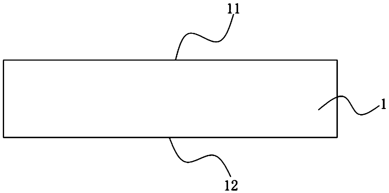
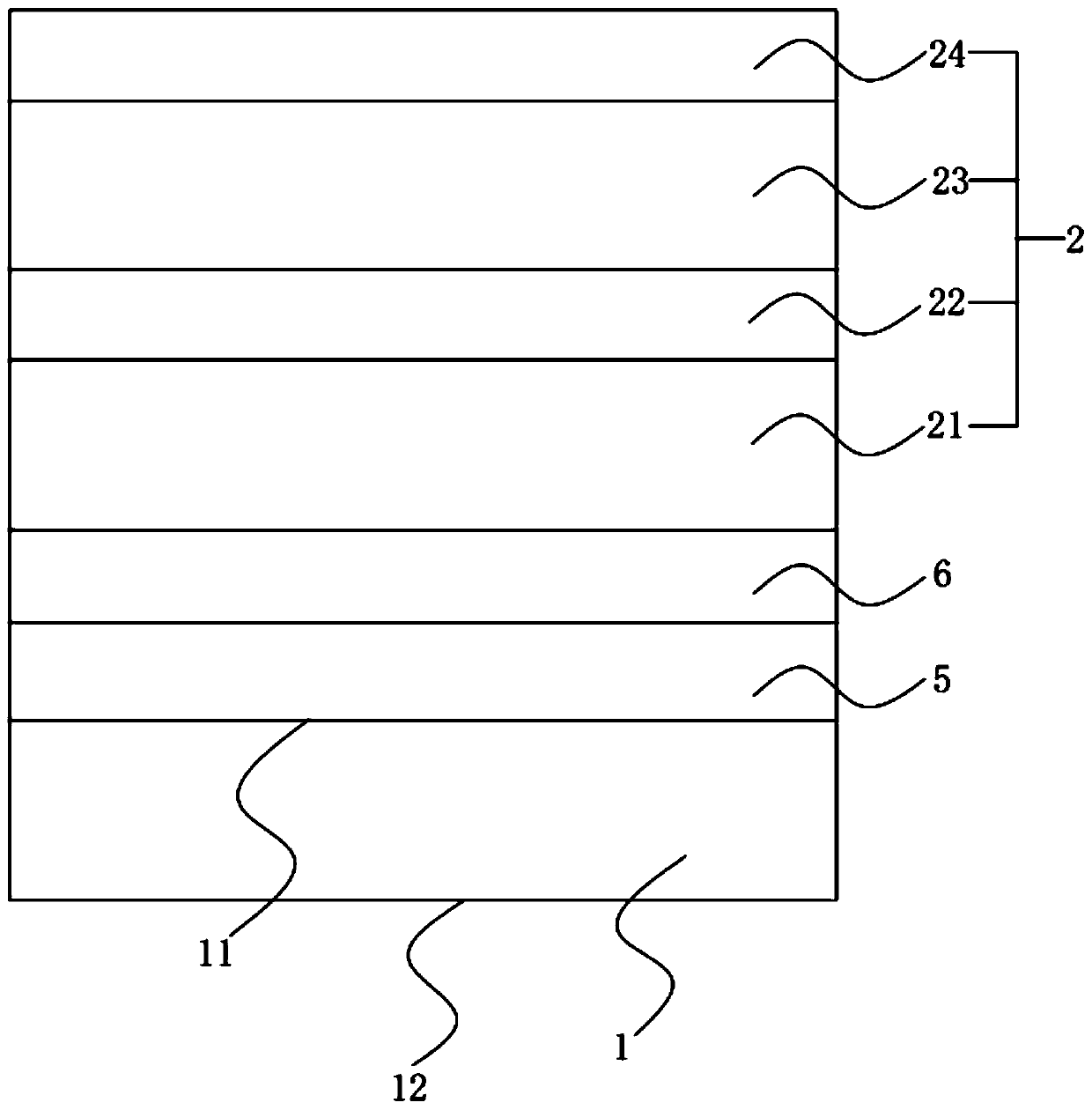
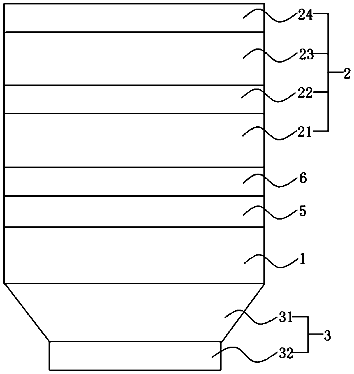
[0050] An embodiment of the present invention provides a crystal epitaxial growth method for preparing a GaInP / GaAs / InGaAs flip-chip triple-junction solar cell. like Figure 1-5 As shown, it specifically includes the following steps:
[0051] Step S1 , forming a lattice matching layer 2 on the first surface 11 of the substrate 1 . Wherein, the lattice constant of the lattice matching layer 2 is the same as that of the substrate 1 .
[0052] In this embodiment, the substrate 1 is selected from but not limited to GaAs, InP, InAs and other substrate materials.
[0053] As a preferred implementation manner, the lattice matching layer 2 includes a first sub-cell layer 21 , a first tunnel junction 22 , a second sub-cell layer 23 and a second tunnel junction 24 . Step S11 comprises the following steps:
[0054] Step S11 , forming a first sub-cell layer 21 on the first surface 11 of the substrate 1 . Wherein, the first sub-cell layer 21 is a GaInP sub-cell layer.
[0055] Step S...
Embodiment 2
[0082] An embodiment of the present invention provides a crystal epitaxial structure, specifically a GaInP / GaAs / InGaAs flip-chip triple-junction solar cell structure. like Figure 1-4 As shown, a substrate 1 , a lattice matching layer 2 , a first lattice mismatching layer 3 and a second lattice mismatching layer 4 are included. in,
[0083] The substrate 1 has an opposite first surface 11 and a second surface 12 , that is, the first surface 11 and the second surface 12 are two surfaces on the substrate 1 facing away from each other. Moreover, the first surface 11 and the second surface 12 are polished surfaces.
[0084] As a preferred embodiment, the thickness of the substrate 1 is 300 μm.
[0085] In this embodiment, the substrate 1 is selected from but not limited to GaAs, InP, InAs and other substrate materials.
[0086] The lattice matching layer 2 and the second lattice mismatching layer 4 are sequentially disposed on the first surface 11 . Wherein, the lattice const...
PUM
 Abstract
Description
Claims
Application Information


