Edge-emitting laser beam shaping structure, laser chip and preparation method of laser chip

An edge-emitting laser and beam shaping technology, which is applied to the structural details of semiconductor lasers, lasers, and laser components, can solve problems such as poor device stability and complex optical path structures, and achieve small divergence angles, high quality, and high power density. Effect

Pending Publication Date: 2019-05-24
TAIYUAN UNIV OF TECH
View PDF10 Cites 8 Cited by
  • Summary
  • Abstract
  • Description
  • Claims
  • Application Information

AI Technical Summary

Problems solved by technology

These methods can realize beam shaping, but these methods design the optical path outside the laser chip for beam shaping. The external optical path shaping method not only has a complicated optical path structure and poor device stability, but also does not increase the beam power density after shaping.

Method used


Image

  • Edge-emitting laser beam shaping structure, laser chip and preparation method of laser chip

Examples


Embodiment Construction

[0026] The present invention will be further described below in conjunction with the accompanying drawings.

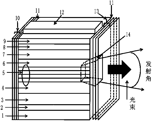
[0027] Such as figure 1 As shown, the present invention has a beam shaping structure of an edge-emitting laser. The beam shaping structure is a trapezoidal platform 14, and the trapezoidal platform 14 is recessed in the N-type doped waveguide layer 4, the active layer 5 and the P-type doped waveguide layer inside the edge-emitting laser chip. In the complex waveguide layer 6, the upper bottom surface of the trapezoidal platform 14 is located on the front output cavity surface of the edge-emitting laser chip, and the surface surrounded by the trapezoidal platform 14 is coated with Si passivation film 11 and anti-reflection film 13 in sequence.

[0028] The length of the upper bottom surface of the trapezoidal platform 14 is 80-120 μm, the width is 1000-1500 Å, and the depth of the trapezoidal platform 14 is 1000-5000 Å. The thickness of the Si passivation film 11 is 10...


PUM


Abstract

The invention discloses an edge-emitting laser beam shaping structure, a laser chip and a preparation method of the laser chip, and belongs to the technical field of semiconductor materials. The invention provides the edge-emitting laser beam shaping structure which improves the power density of laser spots and reduces the beam divergence angle, the laser chip and the preparation method of the laser chip. According to the technical scheme, the side-emitting laser beam shaping structure is a trapezoidal platform, wherein the trapezoidal platform is sunken in an N-type doped waveguide layer, anactive layer and a P-type doped waveguide layer in an edge-emitting laser chip. The upper bottom surface of the trapezoidal table is located on the front output cavity surface of the edge-emitting laser chip, and a Si passivation film and an antireflection film are sequentially disposed on the surface defined by the trapezoidal platform in a plated manner.

Description

technical field [0001] The invention discloses an edge-emitting laser beam shaping structure, a laser chip and a preparation method thereof, belonging to the technical field of semiconductor materials. Background technique [0002] In terms of improving the beam quality of semiconductor lasers, traditional methods mainly include geometric optical shaping methods and diffractive optical shaping methods. At present, the beam shaping methods reported at home and abroad mainly include: cylindrical mirror collimation method, plane mirror shaping technology, aspheric micro-lens shaping technology, micro-chip prism stack shaping method and diffraction element shaping method. These methods can achieve beam shaping, but these methods design the optical path outside the laser chip for beam shaping. The external optical path shaping method not only has a complicated optical path structure and poor device stability, but also does not increase the beam power density after shaping. Cont...

Claims


Application Information

Patent Timeline
Patent Type & Authority Applications(China)
IPC IPC(8): H01S5/00H01S5/02H01S5/32
Inventor 董海亮许并社贾志刚张爱琴屈凯李天保梁建
Owner TAIYUAN UNIV OF TECH
Why Eureka
Try Eureka