PCB welding defect detecting method based on depth information

A technology for PCB board and welding defects, applied in the field of electronic component detection, can solve the problems of slow processing speed, excessive data volume, large false detection rate, etc., to reduce false detection rate, reduce data volume, and low lighting conditions. Effect

Active Publication Date: 2019-05-28
SUZHOU JIANGAO OPTOELECTRONICS TECH
View PDF12 Cites 15 Cited by
  • Summary
  • Abstract
  • Description
  • Claims
  • Application Information

AI Technical Summary

Problems solved by technology

[0002] At present, PCB board defect detection in the industry is mostly based on the two-dimensional color image information of the PCB board. The data volume in the two-dimensional color image is too large and there is a lot of useless information, and the processing speed is slow. Low, high false detection rate, by extracting the color, corner points and other features of the two-dimensional image, and then comparing with the standard board, the defects in the PCB board can be detected

Method used


Image

  • PCB welding defect detecting method based on depth information

Examples


Embodiment Construction

[0020] In order to make the technical means, creative features, goals and effects achieved by the present invention easy to understand, the present invention will be further described below in conjunction with specific embodiments.

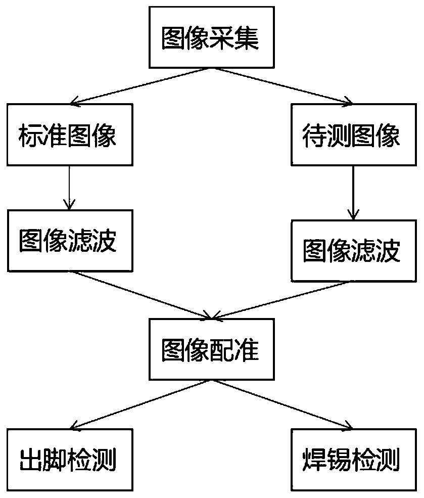
[0021] like figure 1 Shown, a kind of PCB board welding defect detection method based on depth information, described method comprises the following steps:

[0022] Collect the depth data of the welding area of ​​the PCB board to be tested and the welding area of ​​the standard PCB board respectively, use the line laser to scan the front and back of the standard PCB board, and collect the depth data of the front and back sides of the board;

[0023] According to the depth data of the welding area of ​​the two PCB boards, corresponding depth images are generated respectively;

[0024] Obtain the standard welding image according to the depth image of the standard PCB board, obtain the welding image to be tested according to the depth image of the P...


PUM


Abstract

The invention discloses a PCB welding defect detecting method based on depth information. The method comprises the following steps that depth data of a to-be-detected PCB welding area and depth data of a standard PCB welding area are collected respectively; corresponding depth images are generated according to the depth data of the two PCB welding areas respectively; standard welding images are obtained according to standard depth images, and to-be-detected welding images are obtained according to to-be-detected depth images; the standard welding images and the to-be-detected welding images are subjected to image registration; soldering positions are marked in the to-be-detected welding images, and whether or not soldering positions need pin protruding is judged according to ratio operation values of the soldering positions; the registered standard welding images and to-be-detected welding images are subjected to image differentiate operation to obtain binary images; PCB welding defects are determined according to the binary images. The PCB welding defect detecting method based on the depth information has the advantages that the amount of processed data can be reduced, the requirements for illumination conditions are low, and the false detection rate can be reduced.

Description

technical field [0001] The invention relates to the field of detection of electronic components, in particular to a method for detecting welding defects of PCB boards based on depth information. Background technique: [0002] At present, PCB board defect detection in the industry is mostly based on the two-dimensional color image information of the PCB board. The data volume in the two-dimensional color image is too large and there is a lot of useless information, and the processing speed is slow. Low, high false detection rate, by extracting the color, corner points and other features of the two-dimensional image, and then comparing with the standard board, the defects in the PCB board can be detected. Contents of the invention [0003] The purpose of the present invention is to provide a PCB board welding defect detection method based on depth information to solve the above-mentioned multiple defects caused in the prior art. [0004] A method for detecting defects in PC...

Claims


Application Information

Patent Timeline
Patent Type & Authority Applications(China)
IPC IPC(8): G01N21/956G01N21/88G06T7/00
Inventor 林斌汪婷
Owner SUZHOU JIANGAO OPTOELECTRONICS TECH
Why Eureka
Try Eureka