
Power loop testing system for power semiconductor device

A power semiconductor and power cycle technology, applied in the direction of single semiconductor device testing, etc., can solve the problems of affecting test accuracy, narrow application range, prolonging the interval of measuring temperature, etc., to improve test accuracy and reliability, and avoid junction temperature The effect of large fluctuations and reducing the difficulty of control

Pending Publication Date: 2019-05-28
大连芯冠科技有限公司
View PDF0 Cites 11 Cited by
  • Summary
  • Abstract
  • Description
  • Claims
  • Application Information

AI Technical Summary

Problems solved by technology

However, the existing power cycle test system usually uses the method of detecting the parasitic body diode voltage drop to judge the junction temperature of the device under test, so it is necessary to add a reverse small current test
It not only increases the difficulty of system equipment control, but also prolongs the interval of temperature measurement, which makes it impossible to accurately feed back the real-time junction temperature of the device under test; at the same time, the heating is interrupted, resulting in large fluctuations in the junction temperature of the device under test. Affect test accuracy
In addition, the existing power cycle test system is only suitable for devices such as IGBTs or MOSFETs, and cannot test GaN HEMTs, and the scope of application is narrow

Method used


Image

  • Power loop testing system for power semiconductor device
  • Power loop testing system for power semiconductor device
  • Power loop testing system for power semiconductor device

Examples


Embodiment Construction

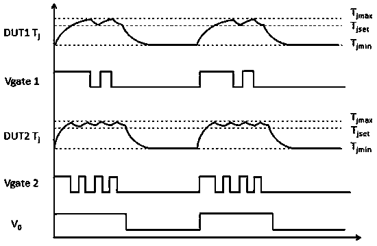
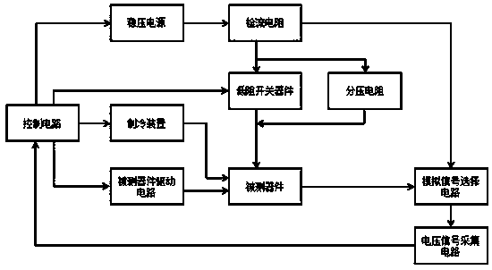
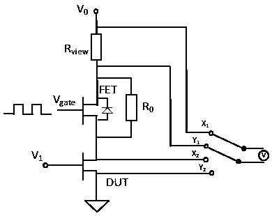
[0010] Power semiconductor device power cycle test system of the present invention such as figure 1 , figure 2 Shown: there are control circuits (single chip microcomputer, etc.) The output V 0 They are respectively connected to multiple detection branches. According to actual needs, each regulated power supply can be connected to 1~40 test branches; the detection branch is equipped with a current-sensing resistor R connected to the regulated power supply. view , with the sense resistor R view in series with the output voltage by the control circuit (V gate ) The low-impedance switching device FET that controls the opening, and the low-impedance switching device FET is connected in parallel with the voltage dividing resistor R 0 , resistor R 0 The resistance value of the FET can be set to 10~1000Ω, which is much higher than the on-resistance of the FET. The sense resistor R view Both ends X1, Y1 are connected with the analog signal selection circuit (CD4052B logic chip...


PUM


Abstract

The invention discloses a power loop testing system for a power semiconductor device. The power loop testing system is provided with a control circuit, stabilized-voltage power sources, refrigerationdevices and tested-device driving circuits, wherein the stabilized-voltage power sources, the refrigeration devices and the tested-device driving circuits are controlled by the control circuit; the output ends of the stabilized-voltage power sources are connected with multiple detection sub-circuits; the detection sub-circuits are provided with current detecting resistors connected with the stabilized-voltage power sources, the current detecting resistors are connected with low-resistance switch devices controlled by the control circuit to be turned on and off in series, the low-resistance switch devices are connected with voltage diving resistors in parallel, the two ends of the current detecting resistors are connected with analog signal select circuits, and the output ends of the analogsignal select circuits are connected with voltage signal collecting circuits; the output ends of the voltage signal collecting circuits are connected with the control circuit; during testing, the tested-device driving circuits are connected with tested-device grids, the low-resistance switch devices are connected with tested devices in series, and the analog signal select circuits are also connected between the sources and the drains of the tested devices.

Description

technical field [0001] The invention relates to a semiconductor device test device, in particular to a power cycle test system for a power semiconductor device with high accuracy, good reliability and wide application range. Background technique [0002] Power semiconductor devices (IGBTs, MOSFETs, GaN HEMTs, etc.), as important devices for power electronics and power conversion, have been widely used in new energy power generation, server power supplies, electric vehicles and other fields. As the core power device of the switching power supply, the reliability of the power semiconductor device directly affects the stability of the system, and the main reason for the reduction of the reliability of the power semiconductor device is the damage during the switching operation. Therefore, how to effectively evaluate the intermittent lifetime of power semiconductor devices is very important. [0003] At present, a power cycle test system has been used to conduct reliability test...

Claims


Application Information

Patent Timeline
IPC IPC(8): G01R31/26
Inventor 任永硕王荣华熊华燕梁辉南高珺
Owner 大连芯冠科技有限公司
Learn More