Wafer adsorption device capable of preventing heat conduction

An adsorption device and heat conduction technology, applied in semiconductor/solid-state device manufacturing, electrical components, circuits, etc., can solve problems such as temperature unevenness and wafer processing, and achieve the effect of reducing contact area, avoiding temperature changes, and reducing pollution

Active Publication Date: 2019-05-28
SHENYANG KINGSEMI CO LTD
View PDF3 Cites 8 Cited by
  • Summary
  • Abstract
  • Description
  • Claims
  • Application Information

AI Technical Summary

Problems solved by technology

[0003] In order to solve the problem of wafer processing caused by uneven temperature, the object of the present invention is to provide a wafer adsorption device that prevents heat conduction

Method used


Image

  • Wafer adsorption device capable of preventing heat conduction
  • Wafer adsorption device capable of preventing heat conduction
  • Wafer adsorption device capable of preventing heat conduction

Examples


Embodiment Construction

[0018] The present invention will be described in further detail below in conjunction with the accompanying drawings.

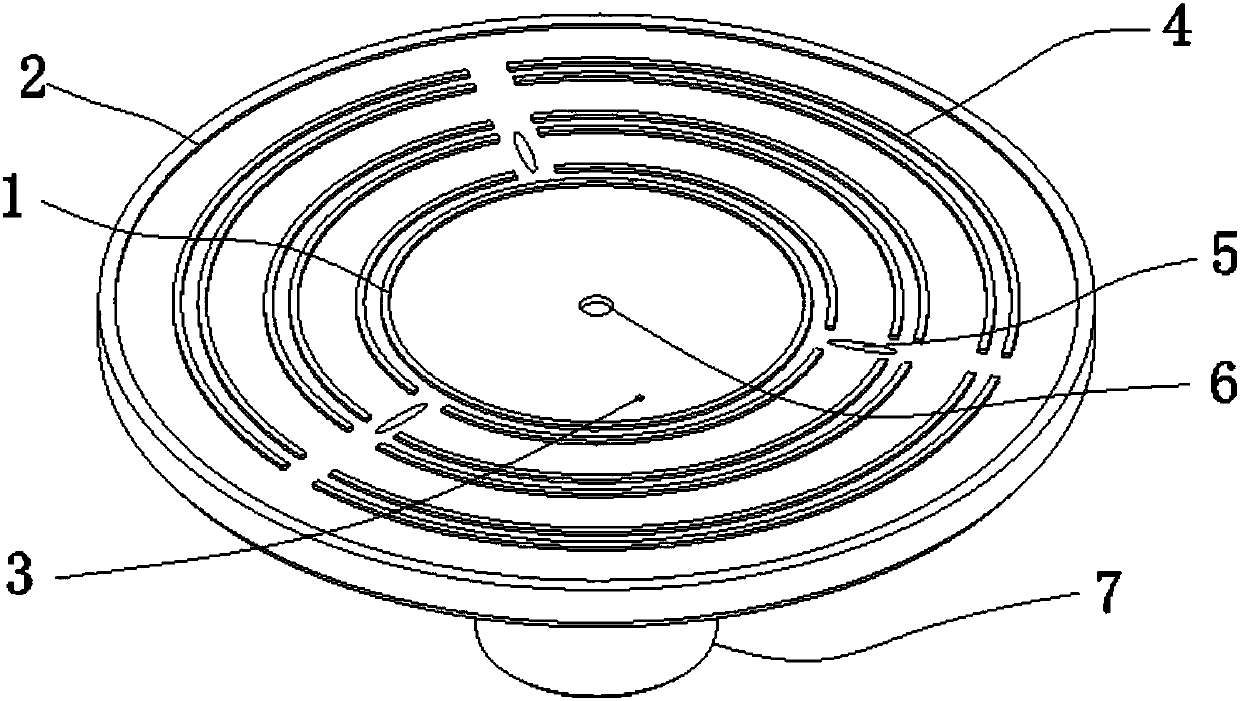
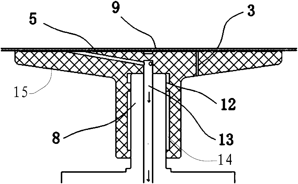
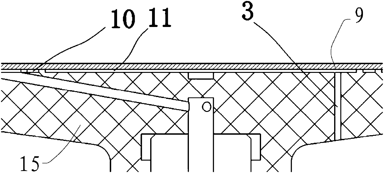
[0019] Such as Figure 1~3 As shown, the present invention includes a wafer carrier 15, which is connected to the motor shaft 8 of the motor, and the wafer 9 is driven to rotate by the motor.

[0020] The axial cross-section of the bearing table 15 is "T" shape, and the lower part of the bearing table 15 is the suction cup neck 7 connected with the motor shaft 8, and the inner hole wall of the suction cup neck 7 is provided with two rings up and down in the axial direction. shaped boss 12, the motor shaft 8 is inserted into the inner hole of the sucker neck 7, and is only connected with the annular boss 12; each annular boss 12 is formed by extending radially inward from the inner hole wall of the sucker neck 7 A non-contact cavity 14 is formed between the other parts of the hole wall except the annular boss 12 and the motor shaft 8 to reduce heat conduction...


PUM


Abstract

The invention belongs to the field of semiconductor production and manufacturing, and particularly relates to a wafer adsorption device capable of preventing heat conduction, an inner sealing ring andan outer sealing ring are respectively arranged on the upper surface of a wafer bearing platform, an annular vacuum cavity is formed between the inner sealing ring and the outer sealing ring, and a normal-pressure cavity is formed in the inner sealing ring; a wafer bearing boss is arranged in the vacuum cavity, and vacuum holes are formed in the wafer bearing boss in the vacuum cavity; a demonstration hole and a normal-pressure cavity exhaust hole are respectively formed in the wafer bearing platform in the normal-pressure cavity; an annular boss is arranged in an inner hole of a suction cupneck on the lower portion of the wafer bearing platform, a motor shaft is inserted from the inner hole of the suction cup neck and only connected with the annular boss, a motor shaft hollow hole is formed in the motor shaft, one end of the vacuum hole communicates with the vacuum cavity, and the other end of the vacuum hole communicates with the motor shaft hollow hole. A wafer is placed on the wafer bearing platform and is supported by the wafer bearing boss, the inner sealing ring and the outer sealing ring, one end of the normal-pressure cavity exhaust hole communicates with the normal-pressure cavity, and the other end communicates with the atmosphere below the wafer bearing platform. The wafer temperature change caused by high-speed rotation of the motor can be effectively avoided.

Description

technical field [0001] The invention belongs to the field of semiconductor production and manufacturing, and is specifically a wafer adsorption device for preventing heat conduction, which can be applied to wafers that require vacuum adsorption for uniform glue, development, glue removal, etching, etc., and then the motor drives the wafer to rotate. in circular processing equipment. Background technique [0002] During the chip manufacturing process, the chemicals on the wafer and its surface are extremely sensitive to temperature changes during the reaction process. In the traditional adsorption device, the high-speed rotation of the motor shaft generates temperature that is directly transmitted upward to the wafer holder near the center, and then transmitted to the wafer through the wafer holder. The temperature distribution of the processed wafer is intermediate heat and radial decline; Uniform, as it can cause issues with wafer processing. Contents of the invention ...

Claims


Application Information

Patent Timeline
Patent Type & Authority Applications(China)
IPC IPC(8): H01L21/683
Inventor 王若愚
Owner SHENYANG KINGSEMI CO LTD
Why Eureka
Try Eureka