A method for preparing periodic graphene pn junctions on n-type 4h/6h-sic silicon surface
A periodic and graphene technology, applied in the field of microelectronic materials, can solve the problems of difficult element doping, complex device structure design, and inability to accurately control the area, and achieve the effect of simple process, inability to accurately control the area, and reduce damage
- Summary
- Abstract
- Description
- Claims
- Application Information
AI Technical Summary
Problems solved by technology
Method used
Image
Examples
Embodiment 1
[0052] A method for preparing periodic graphene PN junctions on an n-type 4H / 6H-SiC silicon surface, comprising the steps of:
[0053] (1) Perform chemical mechanical polishing and chemical cleaning on the off-axis 4° semi-insulating and forward n-type 4H / 6H-SiC silicon surfaces (ie (0001) surface) wafers, and vacuum package them for use; chemical cleaning adopts standard Wet chemical cleaning process.
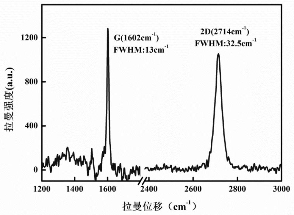
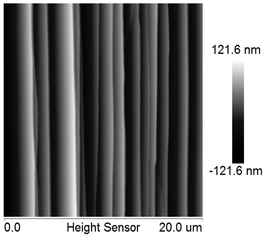
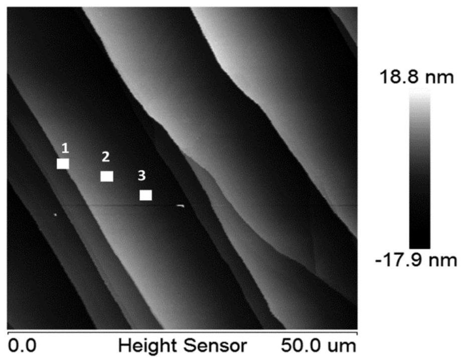
[0054] (2) prepare n-type single-layer graphene on the off-axis 4° semi-insulating SiC wafer, obtain n-type single-layer graphene micro-strips through the stripping step, the steps are as follows:
[0055] Preparation of n-type single-layer graphene: take the off-axis 4° semi-insulating SiC wafer in step (1), place it in the graphite tray in the crucible of the single crystal growth furnace, and evacuate to 10 -7 mbar, heat up to 900°C at a heating rate of 45°C / min, argon gas flow rate of 50 sccm, hydrogen gas flow rate of 25 sccm, hold for 80 min, complete etching, and obtai...
Embodiment 2
[0068] A method for preparing periodic graphene PN junctions on the n-type 4H / 6H-SiC silicon surface, its steps are as described in Example 1, the difference is that in step (3), p-type single-layer graphene is prepared The micro-strip method is:
[0069] Take the forward n-type SiC wafer in step (1), place it in the graphite tray in the crucible of the single crystal growth furnace, adjust the temperature and holding time of the buffer layer growth process and the hydrogen passivation process; buffer layer growth process: temperature 1510 ° C, Holding time 1.5h; hydrogen insertion process: temperature 1000°C, holding time 2.5h; uniform p-type single-layer graphene is formed on the surface of the forward n-type SiC substrate;
[0070] The surface of p-type single-layer graphene is periodically spin-coated with photoresist, the photoresist spin-coating width is 2 μm, and the spin-coating interval is 2 μm. The surface is covered with a photolithography plate and exposed to ultra...
Embodiment 3
[0072] A kind of method that prepares periodic graphene PN junction on n-type 4H / 6H-SiC silicon surface, its step is as described in embodiment 1, difference is, in step (2), the n-type single-layer graphene Preparation process: hydrogen etching process: argon gas flow rate 60 sccm; hydrogen gas flow rate 30 sccm; heating rate is 50 ℃ / min, heating up to 850 ℃, holding for 100 min; graphene growth process: argon gas flow rate 15 sccm, heating rate 3 ℃ / min, the temperature was raised to 1650°C, and the temperature was kept for 1h.
PUM
| Property | Measurement | Unit |
|---|---|---|
| elastic modulus | aaaaa | aaaaa |
Abstract
Description
Claims
Application Information
 - R&D
- Intellectual Property
- Life Sciences
- Materials
- Tech Scout
- Unparalleled Data Quality
- Higher Quality Content
- 60% Fewer Hallucinations
Browse by: Latest US Patents, China's latest patents, Technical Efficacy Thesaurus, Application Domain, Technology Topic, Popular Technical Reports.
© 2025 PatSnap. All rights reserved.Legal|Privacy policy|Modern Slavery Act Transparency Statement|Sitemap|About US| Contact US: help@patsnap.com


