PCB welding spot defect detection method

A defect detection and solder joint technology, applied in the field of image processing, can solve the problems of single feature, small number of experimental samples, single detection type, etc.

Inactive Publication Date: 2019-06-07
GUILIN UNIV OF ELECTRONIC TECH
View PDF8 Cites 22 Cited by
  • Summary
  • Abstract
  • Description
  • Claims
  • Application Information

AI Technical Summary

Problems solved by technology

[0003] Existing PCB solder joint detection methods include: extracting solder joint image features and using Log-Gabor filter for detection, but the classification accuracy is low; combining Bayesian method with SVM, but too many features are extracted, which increases the Computational complexity; the algorithm of probability sorting detects solder joints by analyzing color solder joint images, but this method has a single feature and uses fewer samples; the Hough transform algorithm is used to detect solder joint defects, but the detection type is single; the extraction of solder joints Three-dimensional features, using SFS method for three-dimensional reconstruction, using SVM for classification, the detection accuracy rate is 92.93%, but the classification accuracy rate needs to be improved; the combination of principal component analysis and extreme learning machine fo

Method used


Image

  • PCB welding spot defect detection method
  • PCB welding spot defect detection method
  • PCB welding spot defect detection method

Examples


Example Embodiment

[0032] The specific embodiments of the present invention will be described in more detail below with reference to the schematic diagram. According to the following description and claims, the advantages and features of the present invention will be clearer. It should be noted that the drawings are in a very simplified form and all use imprecise proportions, which are only used to conveniently and clearly assist in explaining the purpose of the embodiments of the present invention.

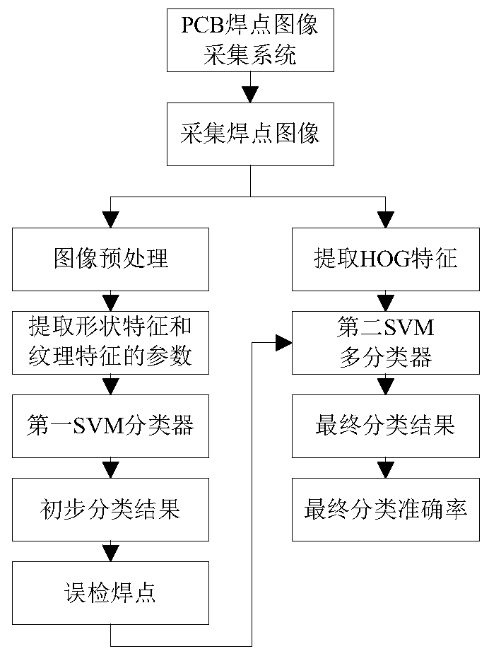
[0033] Such as figure 1 As shown, this embodiment provides a PCB solder joint defect detection method, including:

[0034] S1: Obtain multiple sets of defect feature data corresponding to PCB solder joints, and use SVM algorithm to train to obtain a first SVM classifier based on shape and texture features and a second SVM multi-classifier based on HOG features;

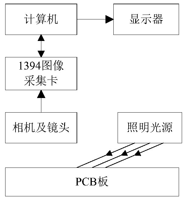
[0035] S2: Obtain a solder joint image of a PCB and preprocess it;

[0036] S3: Extract the shape feature parameters, texture feature parameters...


PUM


Abstract

The invention provides a PCB welding spot defect detection method. Firstly, a welding spot image is preprocessed; shape characteristic parameters and texture characteristic parameters of the welding spots are extracted; the optimal RBF kernel function in SVM classification is adopted to construct the SVM classifier, the second SVM multi-classifier based on HOG features is utilized to obtain the final classification accuracy for false detection of welding spots, the classification accuracy of the method reaches 98.46% or above, and the method has certain superiority.

Description

Technical field [0001] The invention relates to the technical field of image processing, in particular to a method for detecting PCB solder joint defects. Background technique [0002] With the continuous development of the electronics industry, PCB boards are an important part of electronic products, affecting their overall quality and reliability. During the soldering process, PCB solder joints may have defects, causing various problems and losses in electronic products. Therefore, the defect detection of PCB solder joints has become a vital link in the PCB manufacturing process and an important means to ensure quality. [0003] The existing PCB solder joint detection methods include: by extracting the solder joint image features and using the Log-Gabor filter for detection, but the classification accuracy is low; by combining the Bayesian method with SVM, but the extracted features are too many, increasing Computational complexity; Probabilistic sorting algorithm detects solder...

Claims


Application Information

Patent Timeline
IPC IPC(8): G06T7/00G06K9/62
Inventor 陈寿宏张雨璇马峻赵爽侯杏娜郭玲黄新
Owner GUILIN UNIV OF ELECTRONIC TECH
Why Eureka
Try Eureka