Transistor and preparation method thereof, display substrate and display device
What is Al technical title?
Al technical title is built by PatSnap Al team. It summarizes the technical point description of the patent document.
A technology of transistors and substrates, applied in the direction of transistors, semiconductor/solid-state device manufacturing, electric solid-state devices, etc., can solve the problem of shortening the effective channel length, aggravating the influence of short-channel effect threshold voltage uniformity of transistors, and uniformity of transistor threshold voltage To improve the uniformity of the threshold voltage, improve the display quality, and improve the display quality
Pending Publication Date: 2019-06-07
HEFEI XINSHENG OPTOELECTRONICS TECH CO LTD +1
View PDF4 Cites 2 Cited by
Summary
Abstract
Description
Claims
Application Information
AI Technical Summary
This helps you quickly interpret patents by identifying the three key elements:
Problems solved by technology
Method used
Benefits of technology
Problems solved by technology
[0003] However, the short-channel effect of the top-gate oxide semiconductor transistor will affect the uniformity of the threshold voltage of the transistor to a certain extent.
Especially in the conductorization process of the active layer of the transistor, the oxide semiconductor material in the active layer will diffuse into the channel, so that the effective channel length of the transistor is further shortened, which further aggravates the short channel effect of the transistor on its threshold value. Effect of Voltage Uniformity
Method used
Image
Click on the blue label to locate the original text in one second.
Reading with bidirectional positioning of images and text.
Examples
Embodiment Construction
[0046] In order for those skilled in the art to better understand the technical solution of the present invention, a transistor and its manufacturing method, a display substrate and a display device provided by the present invention will be further described in detail below in conjunction with the accompanying drawings and specific embodiments.
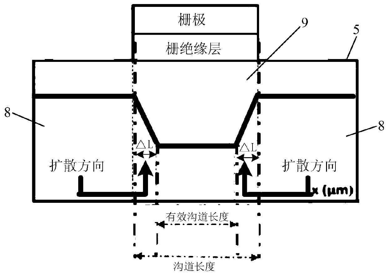
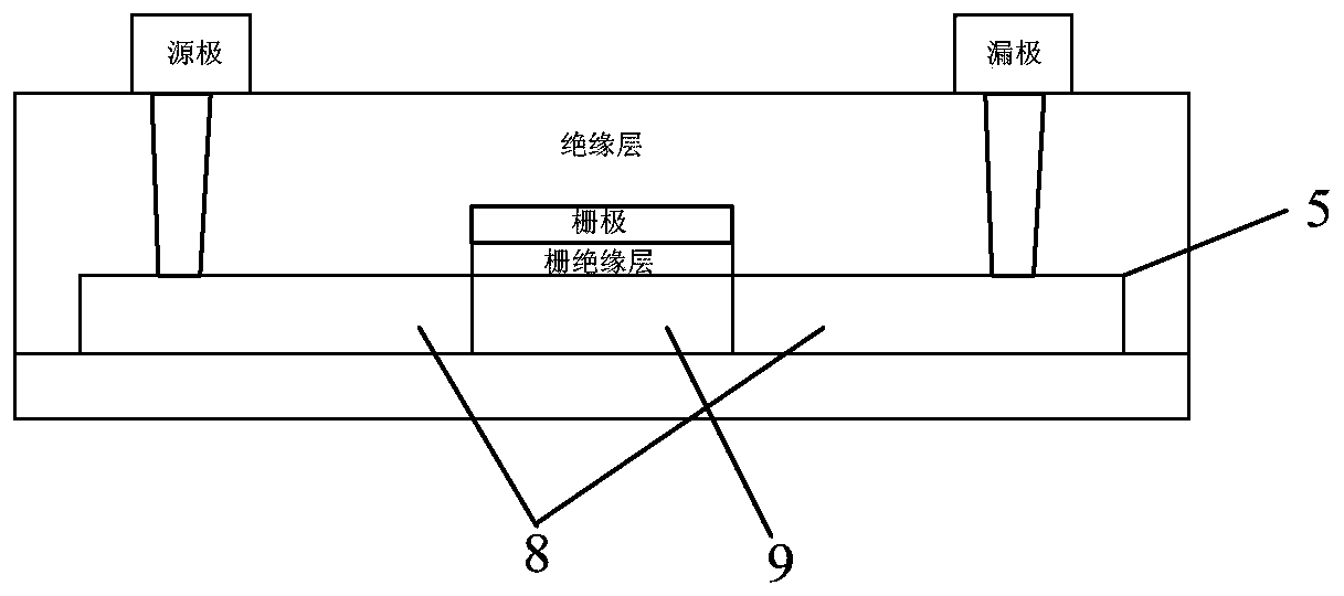
[0047] Since the channel of the top-gate oxide semiconductor transistor is shorter, the uniformity of its threshold voltage is affected by its short-channel effect. Especially in the conductorization process of the active layer of transistor oxide semiconductor material (eg: IGZO), the conductorized regions on the opposite sides of the active layer will have a certain impact on the middle non-conductorized region (effective channel region), Such as in the process of conductorization, such as figure 1 As shown, the oxide semiconductor material in the conductive region 8 on opposite sides of the active layer 5 will diffuse to the middle...
PUM
Abstract
The invention provides a transistor, a preparation method thereof, a display substrate and a display device. The transistor comprises a substrate structure, a gate electrode, a source electrode, a drain electrode and an active layer, wherein the gate electrode, the source electrode, the drain electrode and the active layer are arranged on the substrate structure. The gate electrode, the source electrode and the drain electrode are all located at one side, deviating from the substrate structure, of the active layer. The active layer comprises a first region corresponding to an orthographic projection region of the gate electrode on the substrate structure and a second region located outside the orthographic projection region, wherein the second region is made of a conductive semiconductor material, and the surface, in contact with the first region, of the substrate structure and the surface, in contact with the second region, of the substrate structure are not in the same plane. The surface, in contact with the first region, of the substrate structure and the surface, in contact with the second region, of the substrate structure are not in the same plane, so the transistor enables the height difference to be formed between the first region and the second region of the active layer, and the diffusion path of an active layer material from the second region to the first region in the conductor formation is lengthened, and the diffusion of the active layer material needs greater energy, thereby improving the poor threshold voltage uniformity of the transistor caused by the short-channel effect.
Description
technical field [0001] The present invention relates to the field of display technology, in particular to a transistor and its preparation method, a display substrate and a display device. Background technique [0002] At present, AMOLED products are developing towards high definition, large size and high refresh rate. This puts higher requirements on the thin film transistor (TFT) of the AMOLED driving circuit. Since the top gate (Top Gate) oxide semiconductor transistor can effectively reduce the parasitic capacitance, the refresh frequency is better; and its channel is shorter, the size is smaller, and it can better meet the needs of AMOLED development, so the top gate oxide semiconductor transistor It is a key direction of future research and development. [0003] However, the short-channel effect of the top-gate oxide semiconductor transistor will affect the uniformity of the threshold voltage of the transistor to a certain extent. Especially in the conductorization ...
Claims
Application Information
Patent Timeline
Application Date:The date an application was filed.
Publication Date:The date a patent or application was officially published.
First Publication Date:The earliest publication date of a patent with the same application number.
Issue Date:Publication date of the patent grant document.
PCT Entry Date:The Entry date of PCT National Phase.
Estimated Expiry Date:The statutory expiry date of a patent right according to the Patent Law, and it is the longest term of protection that the patent right can achieve without the termination of the patent right due to other reasons(Term extension factor has been taken into account ).
Invalid Date:Actual expiry date is based on effective date or publication date of legal transaction data of invalid patent.