Wiring area protection method in a touch screen manufacturing process

A production process and wiring area technology, applied in the field of wiring area protection, can solve problems such as disconnection, poor silk screen circuit, no wiring area protection, etc., to achieve the effects of improving production efficiency, saving production costs, and reducing defect rates

Active Publication Date: 2019-06-11
GANZHOU DPT TECH
View PDF14 Cites 0 Cited by
  • Summary
  • Abstract
  • Description
  • Claims
  • Application Information

AI Technical Summary

Problems solved by technology

[0004] However, in the prior art, only the visible area is protected, and the wiring area is not protected
Before the silk screen printing process in the wiring area, due to the many turnover processes of the p

Method used


Image

  • Wiring area protection method in a touch screen manufacturing process
  • Wiring area protection method in a touch screen manufacturing process
  • Wiring area protection method in a touch screen manufacturing process

Examples


Example Embodiment

[0021] Below, the present invention will be further described in conjunction with the accompanying drawings and specific implementation methods. It should be noted that, under the premise of not conflicting, the various embodiments described below or the technical features can be combined arbitrarily to form new embodiments. .

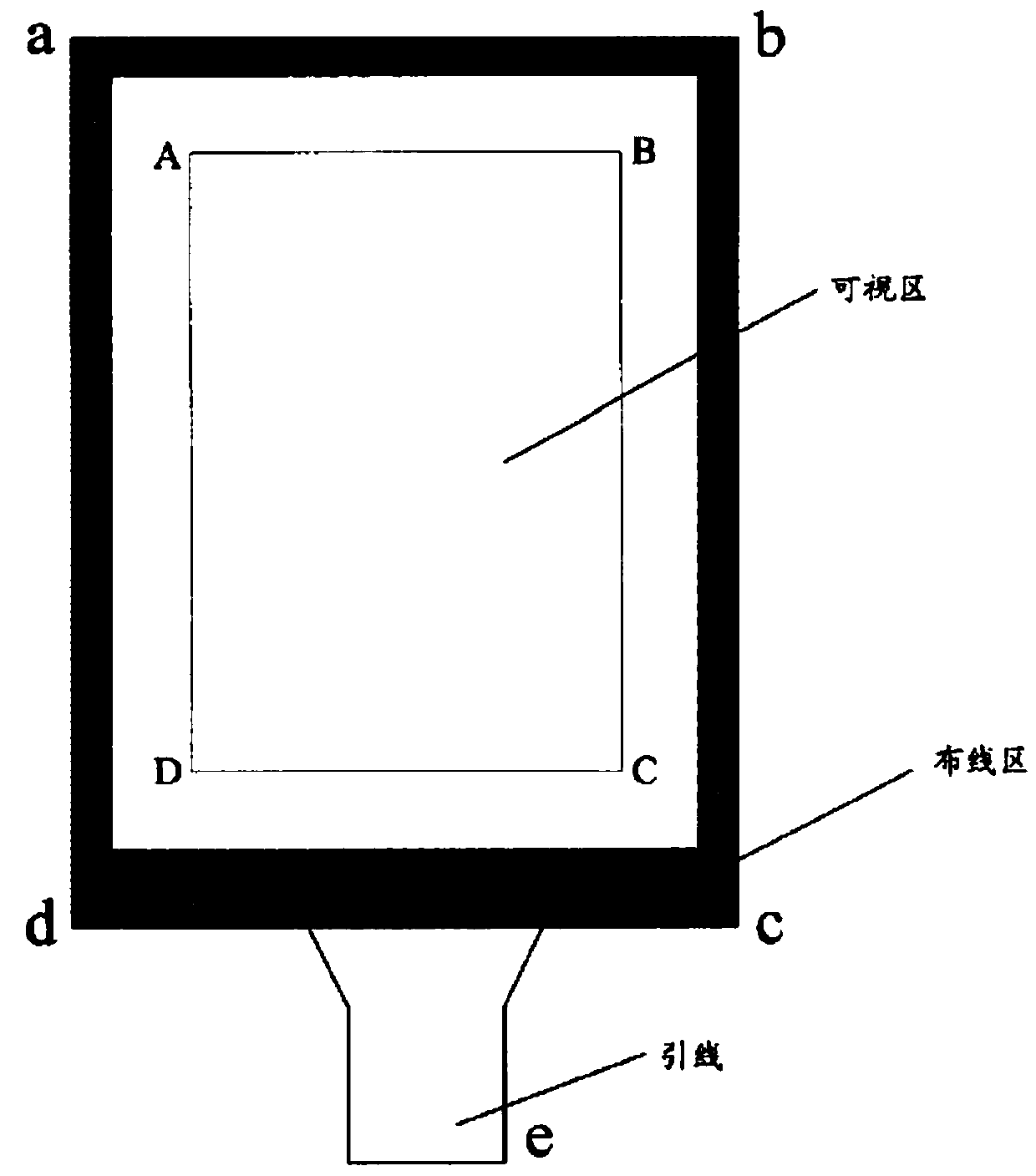
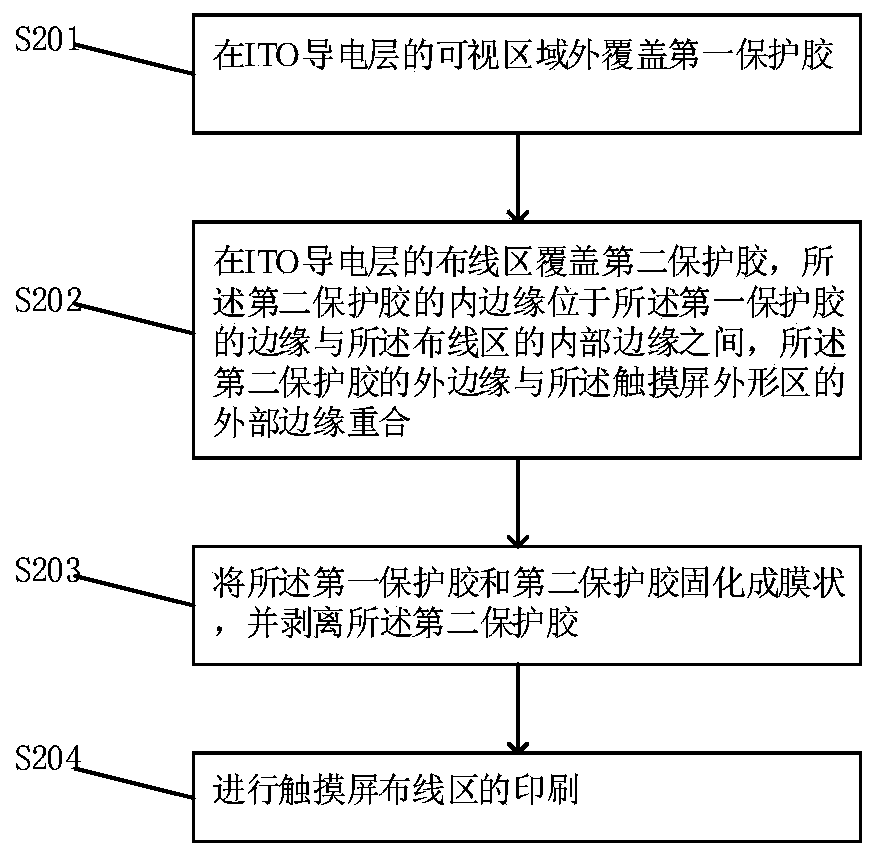
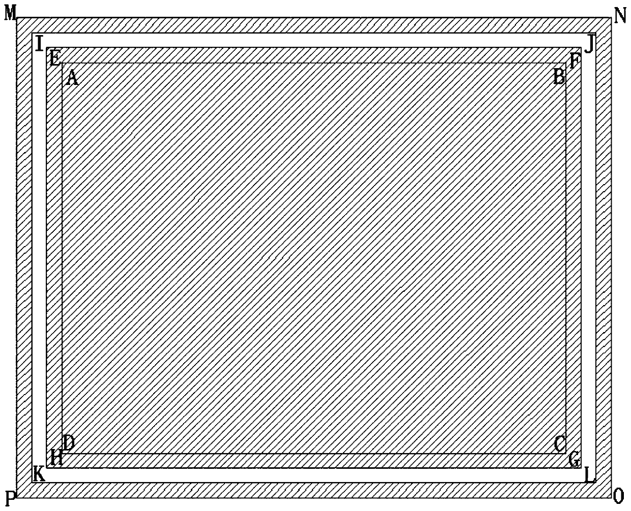
[0022] like figure 2 As described above, in an embodiment of the present invention, a method for protecting a wiring area in a touch screen manufacturing process, the method includes:

[0023] S201, covering the first protective glue outside the visible area of ​​the ITO conductive layer;

[0024] S202. Cover the wiring area of ​​the ITO conductive layer with a second protective glue, the inner edge of the second protective glue is located between the edge of the first protective glue and the inner edge of the wiring area, and the second protective glue The outer edge of the outer edge coincides with the outer edge of the outline area of ​​the touch...


PUM


Abstract

The invention provides a wiring area protection method in a touch screen manufacturing process. The method comprises the steps that a visible area of an ITO conducting layer is covered with first protection glue; covering a wiring area of the ITO conductive layer with a second protective adhesive, the inner edge of the second protective adhesive being located between the edge of the first protective adhesive and the inner edge of the wiring area, and the outer edge of the second protective adhesive being overlapped with the outer edge of the touch screen appearance area; curing the first protective glue and the second protective glue into a film shape, and stripping the second protective glue; And printing a wiring area of the touch screen, and protecting the wiring area of the touch screen.

Description

technical field [0001] The invention relates to the technical field of touch screens, in particular to a method for protecting a wiring area in a manufacturing process of a touch screen. Background technique [0002] figure 1 The structure of the traditional capacitive touch screen and four-wire resistive touch screen is given. The wiring area is located on the four sides of the touch screen. The shaded part abcd in the figure is the wiring area, the middle part ABCD is the visible area, and e is the lead wire of the wiring area . There are many processes in the printing of the wiring area, including silver paste printing, insulating oil printing, transparent oil printing, decorative ink printing, adhesive printing, etc. Such a large number of multi-process printing processes and curing processes will damage or pollute the Indium Tin Oxide (ITO) conductive layer in the visible area, resulting in poor function and appearance such as scratches, dirt, and white spots. [000...

Claims


Application Information

Patent Timeline
IPC IPC(8): G06F3/041
Inventor 张恒军黄培峰谢滨
Owner GANZHOU DPT TECH
Why Eureka
Try Eureka