Memory erasing method and device

A memory and over-erasing technology, which is applied in static memory, read-only memory, information storage, etc., can solve the problems of leakage in non-erased areas and increase the time of over-erased verification operations, so as to reduce leakage current and improve erasure. Effect of removal efficiency, time to reduce

Active Publication Date: 2019-06-11
GIGADEVICE SEMICON (BEIJING) INC
View PDF13 Cites 4 Cited by
  • Summary
  • Abstract
  • Description
  • Claims
  • Application Information

AI Technical Summary

Problems solved by technology

[0005] The present invention provides a memory erasing method and device to solve the problem of increasing the time for over-erasing verification operations due to the leakage of electricity in the non-erased area due to the aging and decay of the memory

Method used


Image

  • Memory erasing method and device
  • Memory erasing method and device
  • Memory erasing method and device

Examples


Embodiment Construction

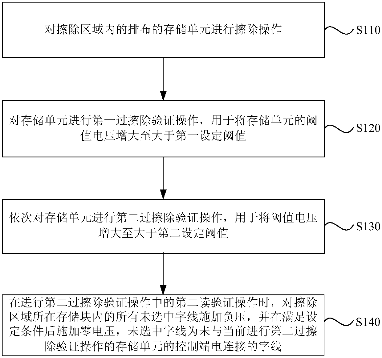
[0024] The present invention will be further described in detail below in conjunction with the accompanying drawings and embodiments. It should be understood that the specific embodiments described here are only used to explain the present invention, but not to limit the present invention. In addition, it should be noted that, for the convenience of description, only some structures related to the present invention are shown in the drawings but not all structures.

[0025] In addition, it should be noted that, for the convenience of description, only parts related to the present invention are shown in the drawings but not all content. Before discussing the exemplary embodiments in more detail, it should be mentioned that some exemplary embodiments are described as processes or methods depicted as flowcharts. Although the flowcharts describe various operations (or steps) as sequential processing, many of the operations may be performed in parallel, concurrently, or simultaneou...


PUM


Abstract

The embodiment of the invention discloses a memory erasing method and device. The memory erasing method comprises the following steps: carrying out erasing operation on memory cells arranged in an erasing area; performing a first over-erase verification operation on the storage unit for increasing the threshold voltage of the storage unit to be greater than a first set threshold; sequentially performing a second over-erase verification operation on the storage unit, wherein the second over-erase verification operation is used for increasing the threshold voltage to be greater than a second setthreshold; when a second read verification operation in the second over-erase verification operation is carried out, applyintg negative voltage to all unselected word lines in the storage block wherethe erase area is located, applying zero voltage after a set condition is met,wherein the unselected word lines are word lines which are not electrically connected with the control end of the storageunit which currently carries out the second over-erase verification operation. According to the technical scheme provided by the embodiment of the invention, the problems of electric leakage of a non-erased area and increase of the time of over-erase verification operation due to aging and decline of the memory can be solved.

Description

technical field [0001] Embodiments of the present invention relate to the technical field of semiconductor storage, and in particular, to a memory erasing method and device. Background technique [0002] When performing an erase (ERASE) operation on a non-volatile memory (for example, NOR-FLASH), the final threshold voltage (Threshold Voltage) of different memory cells will be different, and some memory cells will be over-erased, and also That is, the threshold voltage is lower. In other operations, such as read operation and verify operation, the gate voltage of unselected devices is 0, and there is still leakage current (Leakage Current) for over-erased devices, so that the actual and sense amplifier (Sense Amplifier) The current to be measured compared with the reference current will become larger. When the over-erasing effect is significant or the memory array is large and there are many unselected cells, this situation will be more prominent, and the possibility of dat...

Claims


Application Information

Patent Timeline
Patent Type & Authority Applications(China)
IPC IPC(8): G11C16/34
CPCY02D10/00
Inventor 张赛张建军马向超
Owner GIGADEVICE SEMICON (BEIJING) INC
Why Eureka
Try Eureka