
Integrated optical autocorrelator based on molybdenum selenide double-photon absorption and measuring method

A two-photon absorption and integrated optics technology, which is applied in the direction of instruments, can solve the problems of inability to achieve on-chip integration, poor time resolution, and inability to achieve integration, and achieve the effects of simple structure, full integration, and wide application range

Active Publication Date: 2019-06-14
SHANGHAI JIAO TONG UNIV
View PDF5 Cites 7 Cited by
  • Summary
  • Abstract
  • Description
  • Claims
  • Application Information

AI Technical Summary

Problems solved by technology

[0004] Method 1 is to use the two-photon absorption of silicon detectors combined with the slow light effect of photonic crystals to measure the pulse width. This method requires a row of detector arrays with poor time resolution and can only be used in semiconductor waveguide materials. middle
[0005] Method 2 is to use nanowires or photonic crystal waveguides to generate second harmonics or third harmonics, and observe the harmonic light intensity at different delay positions through a microscope and camera above the waveguide, so as to realize the measurement of pulse width. This method Requires an external microscope and camera and does not allow full on-chip integration
[0006] In short, the above methods have limitations on the waveguide material, or cannot achieve complete on-chip integration. Therefore, an integrated autocorrelation test method that is not clear about the waveguide material and can be fully integrated on-chip is needed.

Method used


Image

  • Integrated optical autocorrelator based on molybdenum selenide double-photon absorption and measuring method
  • Integrated optical autocorrelator based on molybdenum selenide double-photon absorption and measuring method

Examples


Embodiment Construction

[0033] The present invention will be further described below in conjunction with the accompanying drawings and embodiments, but the protection scope of the present invention should not be limited thereby.

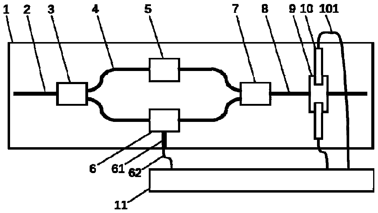
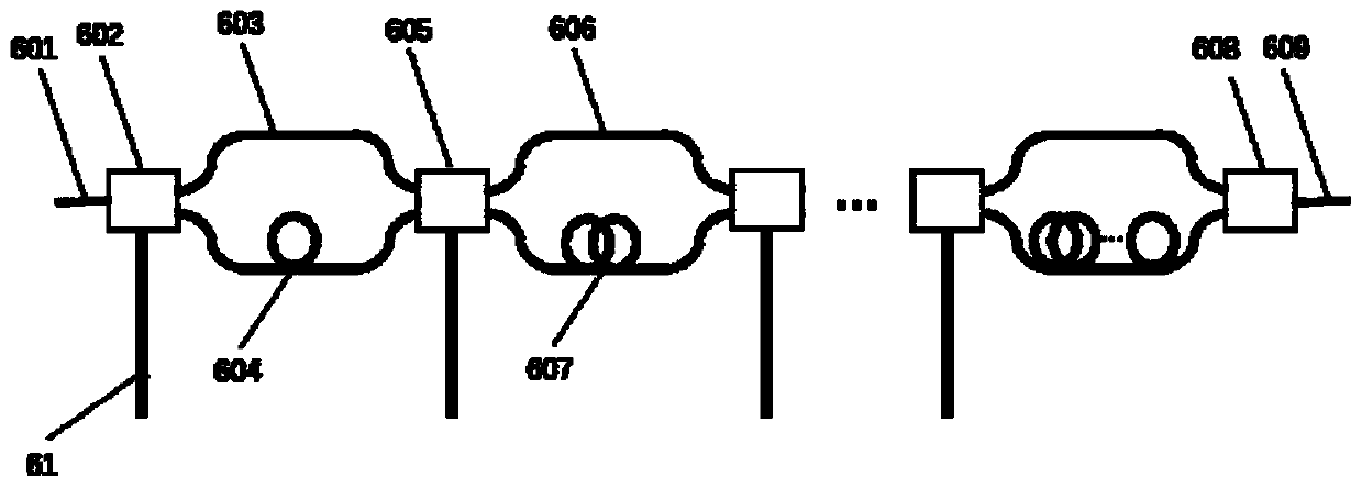
[0034] see first figure 1 , figure 1 It is a structural diagram of the integrated optical autocorrelator device of the present invention, as can be seen from the figure, the composition of the integrated optical autocorrelator device of the present invention is: substrate 1, input waveguide 2, splitter 3, connecting waveguide 4, fixed delay device 5. Adjustable delayer 6, adjustable delayer interface 61, first connector 62, combiner 7, output waveguide 8, molybdenum selenide film 9, on-chip electrode 10, second connector 101 and controller 11. Among them, input waveguide 2, splitter 3, connecting waveguide 4, fixed delayer 5, adjustable delayer 6, adjustable delayer interface 61, combiner 7, output waveguide 8, molybdenum selenide film 9 and on-chip electrodes 10 are pre...


PUM

PropertyMeasurementUnit
Center wavelengthaaaaaaaaaa

Abstract

The invention provides an integrated optical autocorrelator based on molybdenum selenide double-photon absorption and a measuring method. The integrated optical autocorrelator comprises a substrate, an input waveguide, a splitter, a connection waveguide, a fixed time delayer, an adjustable time delayer, an adjustable time delayer interface, a first connector, a combiner, an output waveguide, a molybdenum selenide thin film, an on-chip electrode, a second connector and a controller. According to the integrated optical autocorrelator, on-chip integration of the optical autocorrelator and measurement of the on-chip pulse width can be realized through a simple structure by employing the double-photon absorption characteristic of a molybdenum selenide material.

Description

technical field [0001] The invention relates to integrated pulse width measurement, in particular to an integrated optical autocorrelator and measurement method based on molybdenum selenide two-photon absorption. Background technique [0002] Ultrashort optical pulses are widely used in optical communication, nonlinear optical fiber, optical sensing and other fields. The rise of integrated optics makes ultrashort pulses also play an important role on integrated chips, and the measurement of ultrashort pulses is realized on integrated chips. A better understanding of on-chip pulse characteristics is of great value for various on-chip applications. A key technique is optical autocorrelation measurement, which uses the pulse itself to measure its pulse width. [0003] At present, there are two main methods for realizing pulse autocorrelation measurement on integrated chips: [0004] Method 1 is to use the two-photon absorption of silicon detectors combined with the slow light...

Claims


Application Information

Patent Timeline
IPC IPC(8): G01J11/00
Inventor 吴侃邹卫文李杏陈建平
Owner SHANGHAI JIAO TONG UNIV
Learn More