A Configurable Structure for Optoelectronic Chip Testing

An optoelectronic chip and configuration structure technology, applied in electronic circuit testing, support structure installation, measuring device casing, etc., can solve the problems of strong pertinence, high cost, non-reusability of chips and high-frequency circuits, and achieve reuse. , the packaging time is short, the effect of avoiding the use of

Active Publication Date: 2021-02-12
INST OF SEMICONDUCTORS - CHINESE ACAD OF SCI
View PDF6 Cites 0 Cited by
  • Summary
  • Abstract
  • Description
  • Claims
  • Application Information

AI Technical Summary

Problems solved by technology

[0002] When testing optoelectronic chips, the traditional method is to use gold wire bonding and gold-tin solder for welding and fixing. Although the reliability is strong, it is highly targeted for chips and high-frequency circuits, and the installation process is cumbersome and cannot be reused. It takes a long time and costs high. For optoelectronic chips and high-frequency circuits with different lengths, the test environment needs to be reused many times. The traditional test structure obviously cannot meet the requirements.

Method used


Image

  • A Configurable Structure for Optoelectronic Chip Testing
  • A Configurable Structure for Optoelectronic Chip Testing
  • A Configurable Structure for Optoelectronic Chip Testing

Examples


Embodiment Construction

[0031] In order to make the object, technical solution and advantages of the present invention clearer, the present invention will be described in further detail below in conjunction with specific embodiments and with reference to the accompanying drawings.

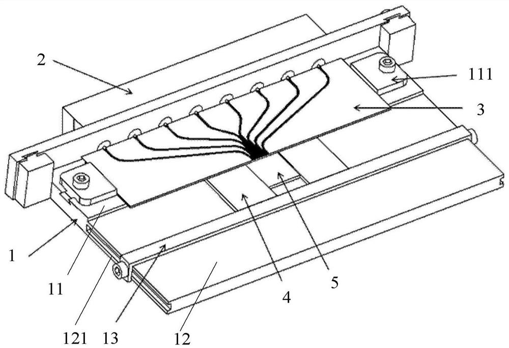
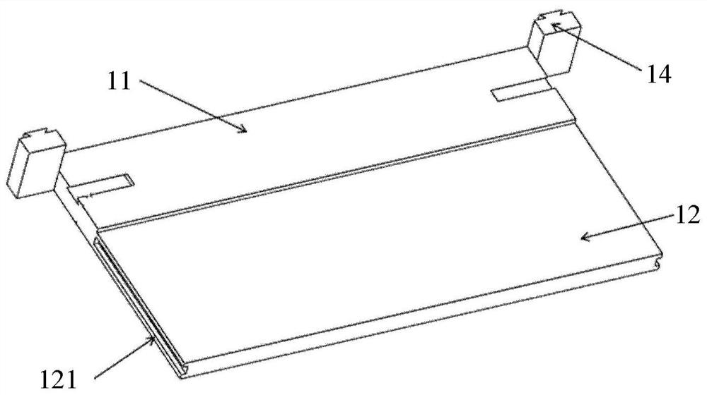
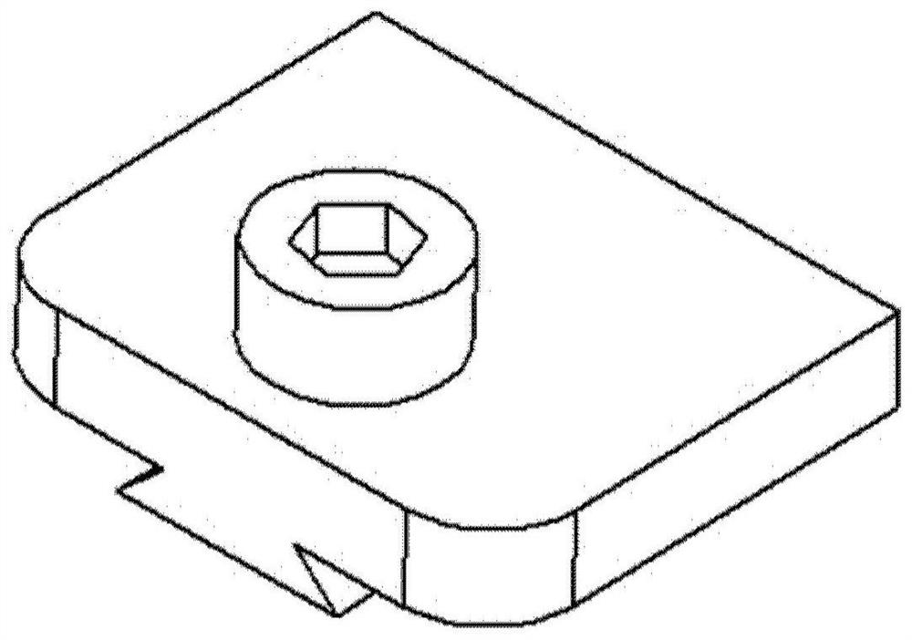
[0032] The present invention provides a configurable structure for optoelectronic chip testing, see figure 1 , including: a carrier plate 1, including a substrate plane 11, a chip plane 12, a chip holder 13 and two fixing seats 14, wherein, the two ends of the substrate plane 11 in the length direction are provided with limiting devices 111, and the two ends of the chip plane 12 in the length direction are provided with There is a slide groove 121, the chip holder 13 is elongated, and the two ends of its length direction are respectively arranged in the slide groove 121, so that the chip holder 13 moves on the chip plane 12, and the substrate plane 11 is parallel to the chip plane 12, And the substrate plane 11 is higher ...


PUM


Abstract

The invention discloses a configurable structure for testing an optoelectronic chip. The configurable structure comprises a carrier plate (1), a joint (2) and a high-frequency circuit board (3), wherein the carrier plate (1) comprises a substrate plane (11), a chip plane (12), a chip fixing frame (13) and two fixed seats (14); the two ends of the substrate plane (11) in the length direction are provided with limiting devices (111); the two ends of the chip plane (12) in the length direction are provided with sliding grooves (121); the chip fixing frame (13) is in a long strip shape; the two ends of the chip fixing frame (13) in the length direction are arranged in the sliding grooves (121) respectively; the two fixed seats (14) are arranged at the end parts of the substrate plane (11) in the length direction; the joint (2) comprises a plurality of insulators (21) and two fixed heads (22); the fixed heads (22) are used in cooperation with the fixed seats (14); and the high-frequency circuit board (3) is arranged on the substrate plane (11), and comprises a circuit heat sink (31), a thin film circuit (32) and a plurality of conductive columns (33). The configurable structure has theadvantages of being detachable, short in manufacturing period, low in cost, wide in suitability and the like.

Description

technical field [0001] The invention relates to the technical field of optoelectronic chips, in particular to a configurable structure for optoelectronic chip testing. Background technique [0002] When testing optoelectronic chips, the traditional method is to use gold wire bonding and gold-tin solder for welding and fixing. Although the reliability is strong, it is highly targeted for chips and high-frequency circuits, and the installation process is cumbersome and cannot be reused. It takes a long time and the cost is high. For optoelectronic chips and high-frequency circuits with different lengths and repeated use of the test environment, the traditional test structure obviously cannot meet the requirements. Contents of the invention [0003] (1) Technical problems to be solved [0004] In view of the above technical problems, the present invention provides a configurable structure for optoelectronic chip testing, which has the advantages of detachable assembly, short...

Claims


Application Information

Patent Timeline
Patent Type & Authority Patents(China)
IPC IPC(8): G01R31/28G01R1/04H05K1/02H05K1/11H05K7/02H05K7/14
Inventor 张志珂韩雪妍赵泽平刘建国
Owner INST OF SEMICONDUCTORS - CHINESE ACAD OF SCI
Why Eureka
Try Eureka