
Preparation method of field effect transistor with n-type doped single crystal diamond field plate structure

A technology of field effect transistors and single crystal diamond, which is applied in semiconductor/solid-state device manufacturing, semiconductor devices, electrical components, etc., can solve problems such as hard breakdown at the edge of electrodes, and achieve increased breakdown voltage, elimination of electric field concentration, and electric field evenly distributed effect

Active Publication Date: 2021-03-02
XI AN JIAOTONG UNIV
View PDF3 Cites 0 Cited by
  • Summary
  • Abstract
  • Description
  • Claims
  • Application Information

AI Technical Summary

Problems solved by technology

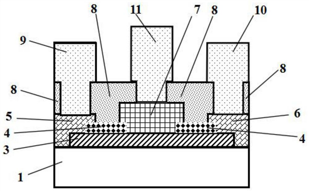
[0005] The purpose of the present invention is to provide a method for preparing a field effect transistor with an n-type doped single crystal diamond field plate structure, so as to solve the problem that the edge of the existing source, gate, and drain electrodes is prone to hard breakdown

Method used


Image

  • Preparation method of field effect transistor with n-type doped single crystal diamond field plate structure
  • Preparation method of field effect transistor with n-type doped single crystal diamond field plate structure
  • Preparation method of field effect transistor with n-type doped single crystal diamond field plate structure

Examples


Embodiment 1

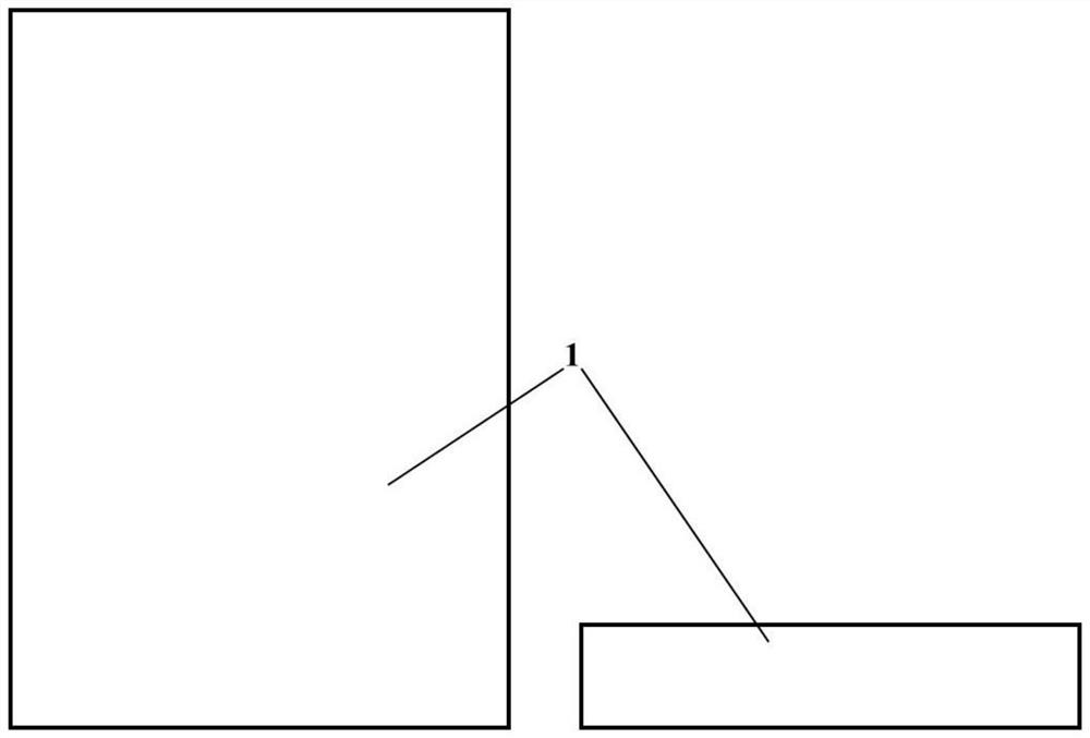
[0050] Step 1: removing the non-diamond phase on the surface of the diamond substrate 1 .

[0051] Such as figure 2 As shown, the diamond substrate 1 is cleaned using a standard acid-base cleaning process to remove the non-diamond phase on the surface, then the diamond substrate 1 is cleaned with alcohol, acetone, and deionized water, and the diamond substrate 1 is dried with nitrogen gas. .

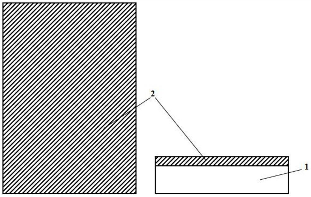
[0052] Step 2: growing a layer of n-type doped single crystal diamond epitaxial thin film 2 on the diamond substrate 1 .

[0053] A 1 μm-thick n-type doped single crystal diamond epitaxial film 2 was grown on a diamond substrate 1 by using microwave plasma chemical vapor deposition technology. The growth conditions were: power 1KW, chamber pressure 50 Torr, total gas flow 500 sccm, phosphine 20 sccm.

[0054] Step 3: Etching the n-type doped single crystal diamond epitaxial film 2 to form a mesa 3 .

[0055] Such as image 3 and Figure 4 As shown, a part of the n-type doped singl...


PUM

PropertyMeasurementUnit
thicknessaaaaaaaaaa
thicknessaaaaaaaaaa
thicknessaaaaaaaaaa

Abstract

The invention discloses a method for preparing a field effect transistor with an n-type doped single-crystal diamond field plate structure. An n-type doped single-crystal diamond epitaxial film is grown on a diamond substrate, and then the n-type doped single-crystal diamond epitaxial film is grown. Etch to form a mesa, deposit two strip-shaped dielectric layers on the mesa, form a drain and a source along the outer edge of the dielectric layer and the mesa, and form a gate between the two dielectric layers to form a field plate structure. The passivation layer covers all structures, removes part of the passivation layer on the source, drain and gate to form via holes, and finally deposits source extraction electrodes, drain extraction electrodes and gate extraction electrodes on the source, drain and gate electrodes along the via holes Electrode; the present invention introduces a field plate structure at the edge of the source, gate and drain electrodes of the diamond MESFET to increase the withstand voltage characteristics of the device, effectively weaken the electric field concentration phenomenon at the source, gate and drain edges of the device, and improve the breakdown voltage performance of the device.

Description

【Technical field】 [0001] The invention belongs to the field of semiconductor devices, in particular to a method for preparing a field effect transistor with an n-type doped single crystal diamond field plate structure. 【Background technique】 [0002] As one of the representatives of ultra-wide bandgap semiconductor materials, diamond has excellent properties incomparable to other semiconductor materials in terms of heat, electricity, sound, light, and machinery. In terms of heat, diamond has high thermal conductivity, low thermal melting, and more significant heat dissipation performance especially at high temperatures. It is an excellent heat sink material for heat dissipation. In recent years, the development of high thermal conductivity diamond film preparation technology has made diamond thermal deposition The application of high-power lasers, microwave devices and integrated circuits has become a reality; in the field of acoustics, diamond has low density and high elast...

Claims


Application Information

Patent Timeline
Patent Type & Authority Patents(China)
IPC IPC(8): H01L21/02H01L21/28H01L21/336
Inventor 王宏兴王艳丰常晓慧王玮宋王振赵丹刘璋成王若铮侯洵
Owner XI AN JIAOTONG UNIV
Learn More