Light emission device and display device using the light emission device as a light source

a technology of light emission device and display device, which is applied in the direction of discharge tube luminescnet screen, discharge tube main electrode, instruments, etc., can solve the problems of high manufacturing cost, additional labor, etc., and achieve the effect of increasing the withstand voltage characteristics of cathode electrodes and gate electrodes, increasing the anode, and high luminan

Inactive Publication Date: 2010-06-10
SAMSUNG SDI CO LTD
View PDF4 Cites 11 Cited by
  • Summary
  • Abstract
  • Description
  • Claims
  • Application Information

AI Technical Summary

Benefits of technology

[0040]In the exemplary embodiments of the present invention, driving can be stabilized by increasing the withstand voltage characteristics of the cathode electrodes and gate electrodes, and high luminance can be achieved by increasing the anode voltage. In addition, since a thick film process for forming an insulation layer and a thin film process for forming gate electrodes may be omitted, the manufacturing process of the light emission device can be simplified, and the manufacturing

Problems solved by technology

Thus, in order to check this, additional labor is requir

Method used


Image

  • Light emission device and display device using the light emission device as a light source
  • Light emission device and display device using the light emission device as a light source
  • Light emission device and display device using the light emission device as a light source

Examples


first embodiment

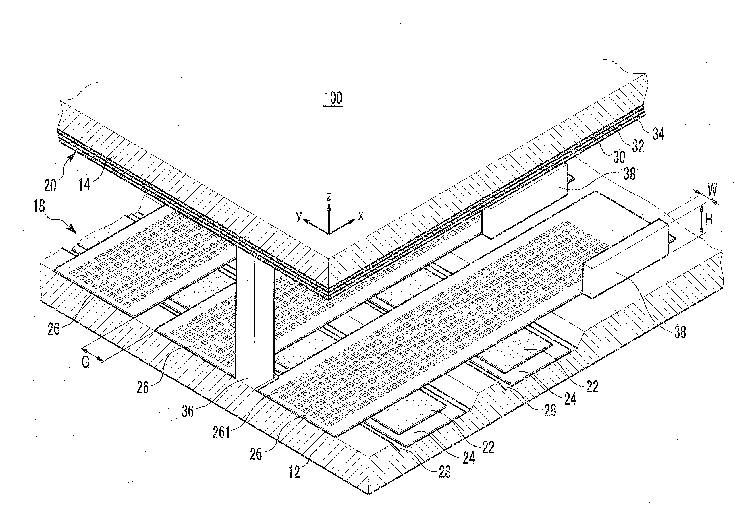
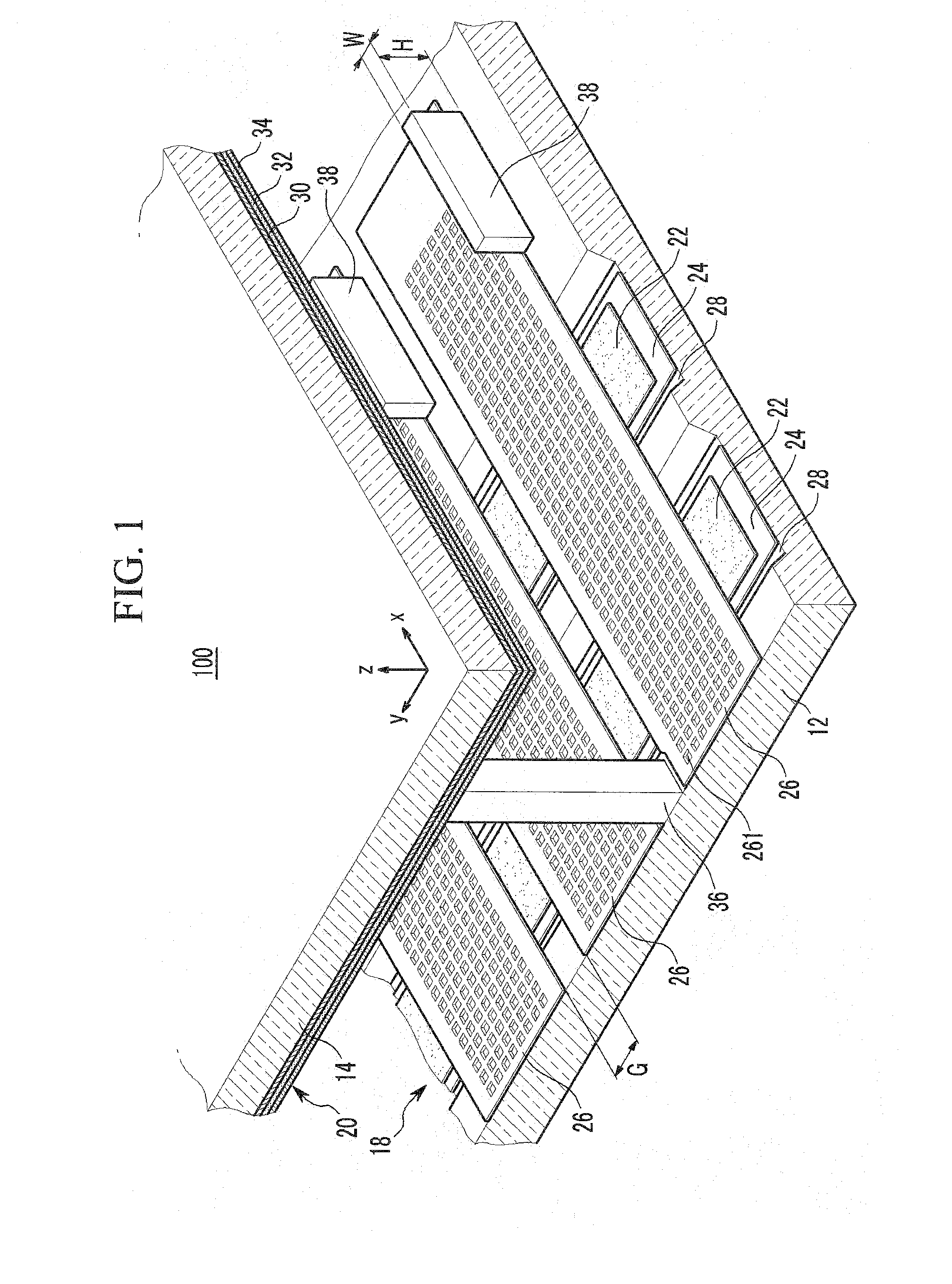
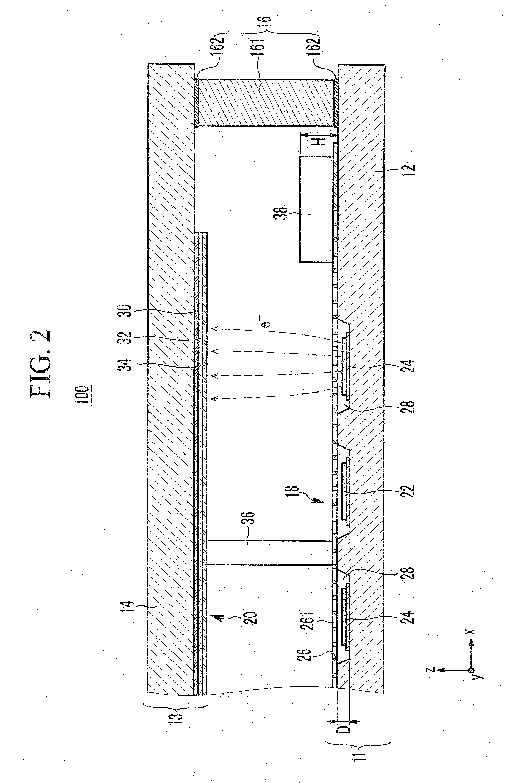
[0053]FIG. 1 and FIG. 2 are, respectively, a schematic perspective view and a schematic cross-sectional view of a light emission device according to the present invention.

[0054]Referring to FIGS. 1 and 2, a light emission device 100 of this embodiment includes an electron discharger 11 and a light emitter 13 that are disposed facing each other. The electron discharger 11 includes a first substrate 12, a plurality of cathode electrodes 24, a plurality of electron emission regions 22, and a plurality of gate electrodes 26. The light emitter 13 includes a second substrate 14 and a light emission unit 20. A sealing member 16 is provided at the peripheries of the first and second substrates 12 and 14 to seal them together, and thus form a vacuum vessel. The interior of the sealed vessel is exhausted to be kept to a degree of vacuum of about 10−6 Torr.

[0055]Of the first and second substrates 12 and 14, the areas disposed inside of the sealing member 16 are divided into an active region su...

second embodiment

[0097]FIG. 6 is a schematic perspective view showing gate electrodes and fixing blocks of the light emission device according to the present invention.

[0098]Referring to FIG. 6, the light emission device of this embodiment has the same configuration as the light emission device of the previous first embodiment except for a structure in which one side of the fixing blocks 381 is fixed to the connection portion 461 located in a widthwise direction (e.g., the y-axis direction of FIG. 6) of the gate electrodes 26. Similar or like members to those of the first embodiment are designated by the same reference numerals.

[0099]The connection portion 461 may be located outside of the second edge portions 26b of the gate electrodes 26, spaced apart a distance, which may be predetermined, from the gate electrodes 26. As the fixing blocks 381 form an integrated structure with the connection portion 461, the installation of the fixing blocks 381 with respect to the first substrate 12 may be easier...

third embodiment

[0100]FIG. 7 is a schematic perspective view showing gate electrodes and fixing blocks of a light emission device according to the present invention.

[0101]Referring to FIG. 7, the light emission device of this embodiment has the same configuration as the light emission device of the previous first embodiment except for a structure in which the top portion of the fixing blocks 382 is fixed to the connection portion 462 located in a widthwise direction (e.g., the y-axis direction of FIG. 7) of the gate electrodes 26. Similar or like members to those of the first embodiment are designated by the same reference numerals.

[0102]In this embodiment, since the connection portion 462 is located overlapping with part of the gate electrodes 26, the fixing blocks 382 and the connection portion 462 are located in the inactive area. As the fixing blocks 382 form an integrated structure with the connection portion 462, the installation of the fixing blocks 382 with respect to the first substrate 12...


PUM


Abstract

A light emission device including an electron discharger including a first substrate, a plurality of cathode electrodes, a plurality of electron emission regions, and a plurality of gate electrodes, the first substrate having a plurality of recessed portions at a first surface of the first substrate, the cathode electrodes extending along a first direction and in the recessed portions, the electron emission regions on the cathode electrodes, and the gate electrodes extending along a second direction crossing the first direction; a light emitter including a second substrate, the second substrate having a second surface facing the first surface of the first substrate with a gap therebetween; and a plurality of fixing blocks on the first substrate and between the gate electrodes, the fixing blocks being separated from the light emitter.

Description

CROSS-REFERENCE TO RELATED APPLICATION[0001]This application claims priority to and the benefit of U.S. Provisional Patent Application No. 61 / 119,977 filed, Dec. 4, 2008, the entire content of which is incorporated herein by reference.BACKGROUND OF THE INVENTION[0002]1. Field of the Invention[0003]The present invention relates to a light emission device. More particularly, the present invention relates to an electron emission unit of a light emission device. Furthermore, the present invention relates to a display having a light emission device.[0004]2. Description of the Related Art[0005]A light emission device typically has a front substrate on which a phosphor layer and an anode electrode are formed and a rear substrate on which electron emission regions and driving electrodes are formed. The peripheries of the front and rear substrates are bonded together by a sealing member to form a sealed interior space, and then the interior space is exhausted, thereby forming a vacuum vessel...

Claims


Application Information

Patent Timeline
IPC IPC(8): G02F1/13357H01J1/54G09F13/08
CPCH01J63/02H01J1/30
Inventor RYU, KYUNG-SUNSEON, HYEONG-RAECHANG, DONG-SU
Owner SAMSUNG SDI CO LTD
Why Eureka
Try Eureka