N-type diamond-doped field effect transistor with field plate structure

A field effect transistor, diamond technology, applied in semiconductor devices, electrical components, circuits, etc., can solve problems such as hard breakdown of electrode edges, and achieve the effects of increasing breakdown voltage, increasing withstand voltage characteristics, and eliminating electric field concentration.

Pending Publication Date: 2019-05-17
XI AN JIAOTONG UNIV
View PDF0 Cites 4 Cited by
  • Summary
  • Abstract
  • Description
  • Claims
  • Application Information

AI Technical Summary

Problems solved by technology

[0005] The purpose of the present invention is to provide a field effect transistor with an n-type doped diamond field plate structure to solve the problem that the edge of the existing source, gate, and drain electrodes is prone to hard breakdown

Method used


Image

  • N-type diamond-doped field effect transistor with field plate structure
  • N-type diamond-doped field effect transistor with field plate structure
  • N-type diamond-doped field effect transistor with field plate structure

Examples


Embodiment Construction

[0028] The present invention will be described in detail below with reference to the drawings and specific embodiments.

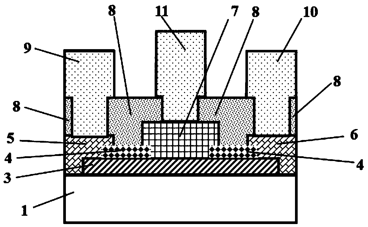
[0029] The invention discloses a field effect transistor with an n-type doped diamond field plate structure, such as figure 1 As shown, it includes a diamond substrate 1. On the diamond substrate 1, a mesa 3 formed by an n-type doped single crystal diamond epitaxial film 2 is laid. On the mesa 3, two strip-shaped dielectric layers 4 are laid along each dielectric layer. Drain 6 and source 5 are laid on the outer edges of 4 and mesa 3, and a gate 7 is laid between two dielectric layers 4. The dielectric layer 4, drain 6, source 5 and gate 7 form a field plate Structure, source 5, drain 6 and gate 7 are respectively deposited with active extraction electrode 9, drain extraction electrode 10 and gate extraction electrode 11, the source extraction electrode 9, drain extraction electrode 10 and gate extraction electrode 11 pass blunt The layers 8 are completely sep...


PUM


Abstract

The present invention discloses a n-type diamond-doped field effect transistor with a field plate structure. The field effect transistor comprises a diamond substrate; a mesa formed by n-type monocrystal diamond-doped epitaxial film is laid on the diamond substrate; two strip-shaped dielectric layers are deposited on the mesa; a drain and a source are respectively laid along the outer edges of each dielectric layer and the mesa; a gate is laid between the two dielectric layers; and the dielectric layers, the drain, the source and the gate constitute a field plate structure. A source extractionelectrode, a drain extraction electrode and a gate extraction electrode are respectively deposited on the source, the drain and the gate; and the source extraction electrode, the drain extraction electrode and the gate extraction electrode are completely separated from each other by a passivation layer. The invention introduces the field plate structure at the edges of the source, gate and drainelectrodes of the diamond MESFET, effectively reduces the electric field concentration effect, increases the breakdown characteristics of the device, effectively reduces the electric field concentration phenomena at the edges of the source, the gate and the drain of the device and improves the breakdown voltage of the device.

Description

【Technical Field】 [0001] The invention belongs to the field of semiconductor devices, and particularly relates to a field effect transistor with an n-type doped diamond field plate structure. 【Background technique】 [0002] As one of the representatives of ultra-wide bandgap semiconductor materials, diamond has excellent performance incomparable to other semiconductor materials in terms of heat, electricity, sound, light, and machinery. In terms of heat, diamond has high thermal conductivity, low heat fusion, and more significant heat dissipation efficiency at high temperatures. It is an excellent heat sink material for heat dissipation. In recent years, the development of high thermal conductivity diamond film preparation technology has made diamond thermal deposition Applications in high-power lasers, microwave devices and integrated circuits have become a reality; in the field of acoustics, diamond has low density and high elastic modulus. These characteristics enable diamond ...

Claims


Application Information

Patent Timeline
Patent Type & Authority Applications(China)
IPC IPC(8): H01L29/40H01L29/78
Inventor 王宏兴王艳丰常晓慧王玮宋王振赵丹刘璋成王若铮侯洵
Owner XI AN JIAOTONG UNIV
Why Eureka
Try Eureka