Eureka AIR delivers breakthrough ideas for toughest innovation challenges, trusted by R&D personnel around the world.

Chip-level package multi-face light-emitting LED and packaging method thereof, and backlight module

A chip-level packaging, multi-faceted light-emitting technology, applied in electric light sources, lighting devices, light source fixing and other directions, can solve the problems of high cost, poor effect, adding optical lenses, etc., to achieve cost reduction, large light-emitting angle, and eliminating the need for mounting The effect of labor cost

Inactive Publication Date: 2019-06-18
HUIZHOU JUFEI OPTOELECTRONICS CO LTD
View PDF5 Cites 3 Cited by
  • Summary
  • Abstract
  • Description
  • Claims
  • Application Information

AI Technical Summary

Problems solved by technology

[0006] The chip-level packaged multi-faceted light-emitting LED and its packaging method and backlight module provided by the present invention mainly solve the technical problem of solving the problems of high cost and poor effect of adding an optical lens to the existing CSP LED application

Method used


Image

  • Chip-level package multi-face light-emitting LED and packaging method thereof, and backlight module
  • Chip-level package multi-face light-emitting LED and packaging method thereof, and backlight module
  • Chip-level package multi-face light-emitting LED and packaging method thereof, and backlight module

Examples


Embodiment 1

[0049] In order to solve the problem that an optical lens needs to be added to the existing CSP LED application, the cost is high, and the effect is poor, this embodiment provides a new packaging method for a multi-faceted light-emitting LED. The LED obtained by this packaging method does not need to add an optical lens when used. The cost is low and the effect is good.

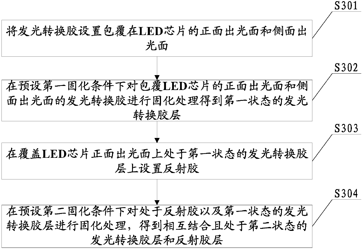
[0050] see image 3 As shown, the multi-faceted light-emitting LED packaging method provided in this embodiment includes:

[0051] S301: Covering the front light-emitting surface and the side light-emitting surface of the LED chip with a light-emitting conversion glue.

[0052] A general LED chip has four sides, and each side is a light-emitting surface, and the top surface is a front surface, which is also a light-emitting surface. Therefore, a general LED chip has a side light emitting surface and a front light emitting surface. The current LEDs are mainly used on the front light-emitting surface of the ...


PUM


Abstract

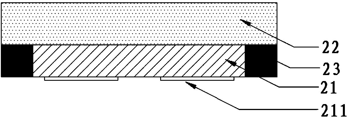
The invention provides a chip-level package multi-face light-emitting LED and a packaging method thereof, and a backlight module. The method comprises the following steps of firstly setting and curinga luminescent conversion adhesive coating the front light-emitting surface and the side light-emitting surface of the LED chip; forming and curing a reflective adhesive coating a luminescent conversion adhesive layer in the first state on the front light-emitting surface of the LED chip to obtain a fluorescent adhesive layer and a reflective adhesive layer which are combined with each other and in the second state; reflecting the obtained light emitted from the front light-emitting surface of the LED by a reflective adhesive layer through the luminescent conversion adhesive layer, and emitting the light from the side light-emitting surface of the LED such that the light generated by the LED is emitted from the side light-emitting surface of the LED. Compared with the existing LED emittedfrom the front light-emitting surface, the light-emitting angle is larger and the light mixing effect is better, thereby when used in the backlight field without using an optical lens, eliminating thehardware cost of the optical lens and the labor cost of the mounting and enhancing the light mixing effect while greatly reducing the backlight cost.

Description

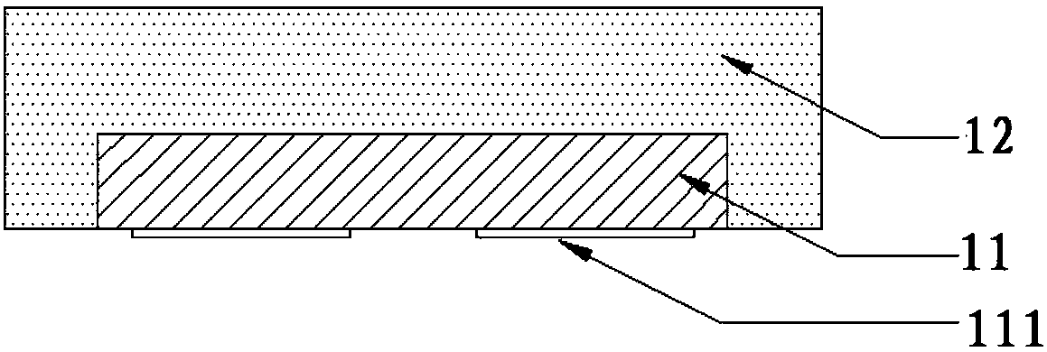
technical field [0001] The present invention relates to the field of LED (Light Emitting Diode, light-emitting diode), in particular to a chip-level packaged multi-faceted light-emitting LED, a packaging method thereof, and a backlight module. Background technique [0002] With the application and development of LEDs, the size requirements of LEDs are getting smaller and smaller. In order to meet the requirements of reducing the size of LEDs, Chip Scale Package (CSP) LEDs have emerged. The current CSP LEDs mainly have two structures: [0003] One is five-side emitting CSP LED, see figure 1 As shown, the structural principle is that after the fluorescent adhesive layer 12 is molded on the flip-chip LED chip 11 (FlipLED chip), the finished product is cut to obtain a single CSP LED. The four sides and the front of the top are light-emitting surfaces, and the bottom Electrodes 111 are provided on the back side. The disadvantage of this structure is that the light angle is rel...

Claims


Application Information

Patent Timeline
Patent Type & Authority Applications(China)
IPC IPC(8): H01L33/54H01L33/50H01L33/60F21S8/00F21V19/00
Inventor 魏冬寒孙平如邢其彬
Owner HUIZHOU JUFEI OPTOELECTRONICS CO LTD
Why Eureka
Eureka Blog
Learn More