level shift circuit suitable for a GaN high-speed gate drive circuit

A technology of level shifting circuit and gate driving circuit, which is applied in the direction of logic circuit coupling/interface, logic circuit connection/interface layout, electrical components, etc. using field effect transistors, to improve reliability, reduce transmission delay, and high CMTI capability Effect

Active Publication Date: 2019-06-18
UNIV OF ELECTRONICS SCI & TECH OF CHINA
View PDF7 Cites 13 Cited by
  • Summary
  • Abstract
  • Description
  • Claims
  • Application Information

AI Technical Summary

Problems solved by technology

[0005] Aiming at the requirements of the gate drive of GaN power switching devices on transmission speed, anti-common-mode transient noise interference capability and rail-to-rail output capability, and the shortcomings that traditional level shift circuits cannot be applied to the gate drive of GaN power switching devices, the present invention proposes a A high-speed level-shifting circuit, which can realize the anti-switching node voltage V in the half-bridge hard switching driving application of GaN power switching devices under the condition that the level-shifting circuit is guaranteed to realize ultra-low transmission delay SW for negative rail-to-rail output capability (at typical V SW =-2.5~-3V DC voltage can still achieve rail-to-rail output), and can achieve high immunity to common-mode transient noise interference (CMTI=50V / ns), suitable for GaN power switching devices half-bridge hardware switch drive application

Method used


Image

  • level shift circuit suitable for a GaN high-speed gate drive circuit
  • level shift circuit suitable for a GaN high-speed gate drive circuit
  • level shift circuit suitable for a GaN high-speed gate drive circuit

Examples


Embodiment Construction

[0051] The technical scheme of the present invention is described in detail below in conjunction with accompanying drawing and specific embodiment:

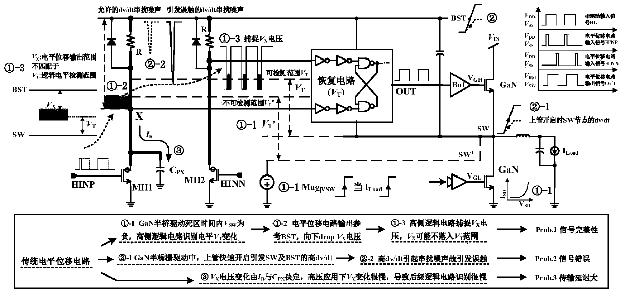
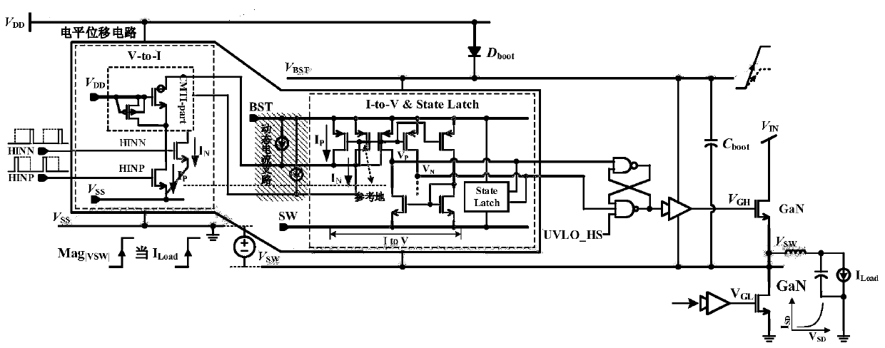
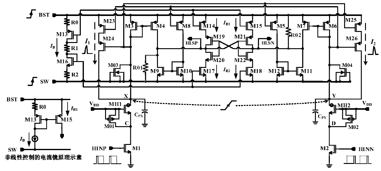
[0052] The present invention considers: 1. Under the rail-to-rail output requirement, when the GaN gate drive circuit enters the dead time, the power switch node voltage V SW is a negative value, and the chip voltage range is the chip internal power supply V DD to chip ground V SS , the negative voltage has been separated from the lowest voltage of the front-end circuit, so the level shift circuit wants to achieve rail-to-rail output (especially to generate a voltage of V SW Logical low signal), the traditional method of only using voltage signals for transmission cannot be used; 2. Under the requirements of high voltage applications, the parasitic capacitance in the withstand voltage area of ​​the high withstand voltage tube will elongate the voltage change speed, so the high withstand voltage tube is located The branch circui...


PUM


Abstract

The invention discloses a level shift circuit suitable for a GaN high-speed gate drive circuit, and belongs to the technical field of power management. Gate drive control signal transmission is carried out by using a voltage-to-current-to-voltage structure, so that the rail-to-rail output capability is realized, and the situation of signal delay and even loss caused by the fact that the voltage ofa switch node of the GaN high-speed gate drive circuit is negative in dead time can be prevented; A dynamic current branch is adopted to carry out fast voltage transient protection, a common-mode transient noise interference resisting module is adopted to carry out anti-floating power supply rail dv/dt crosstalk protection, and the high CMTI capacity of an input end and an intermediate node of alevel shift circuit is achieved. A positive feedback latch module for limiting current is used for latching the current as an output maintaining structure. According to the level shift circuit, the transmission delay of the level shift circuit is reduced, high-speed signal transmission is realized, a low-resistance access and positive feedback are provided to prevent circuit output from being interfered by high dv/dt capability of the floating power supply rail, so that the high CMTI capability of the output end of the level shift circuit is realized, and the reliability of the circuit is improved.

Description

technical field [0001] The invention belongs to the technical field of power management, and in particular relates to a level shift circuit suitable for a GaN high-speed gate drive circuit. Background technique [0002] Since GaN power switching devices (such as GaN HEMT) have low gate charge Qg, low on-resistance R ds_on , high voltage resistance, no reverse recovery time and other good device physical characteristics, GaN power switching device high voltage half-bridge hard switching drive technology in high frequency, high power density power conversion applications (such as half bridge, full school, synchronous rectification BUCK converter, etc. ) becomes more and more important. High-speed, low power consumption, high CMTI (Common Mode Transient Immunity, ability to resist common mode transient noise interference) level shift circuit is very critical in the high-side drive circuit of the GaN power switching device drive circuit, because it determines the high-side Dri...

Claims


Application Information

Patent Timeline
Patent Type & Authority Applications(China)
IPC IPC(8): H03K17/687H03K19/0185
Inventor 明鑫张宣张志文范子威胡黎潘溯秦尧王卓张波
Owner UNIV OF ELECTRONICS SCI & TECH OF CHINA
Why Eureka
Try Eureka