Non-contact type ridge waveguide, micro-strip and coupling slot probe transition circuit

A non-contact, ridged waveguide technology, applied in circuits, waveguide devices, electrical components, etc., can solve problems such as operating bandwidth limitations, achieve low-loss transition, strong electric field signals, and avoid effects.

Active Publication Date: 2019-06-21
10TH RES INST OF CETC
View PDF4 Cites 8 Cited by
  • Summary
  • Abstract
  • Description
  • Claims
  • Application Information

AI Technical Summary

Problems solved by technology

Since the penetrating mechanism is not in direct contact with the back of the waveguide, the strength of the coupl

Method used


Image

  • Non-contact type ridge waveguide, micro-strip and coupling slot probe transition circuit
  • Non-contact type ridge waveguide, micro-strip and coupling slot probe transition circuit
  • Non-contact type ridge waveguide, micro-strip and coupling slot probe transition circuit

Examples


Embodiment Construction

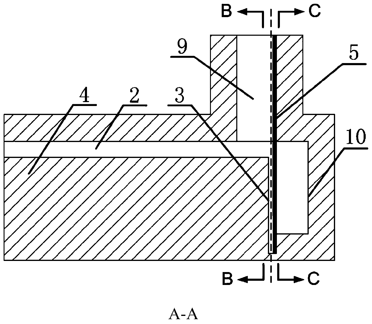
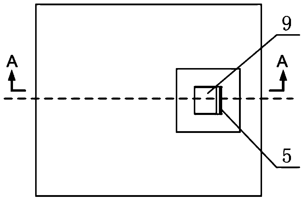
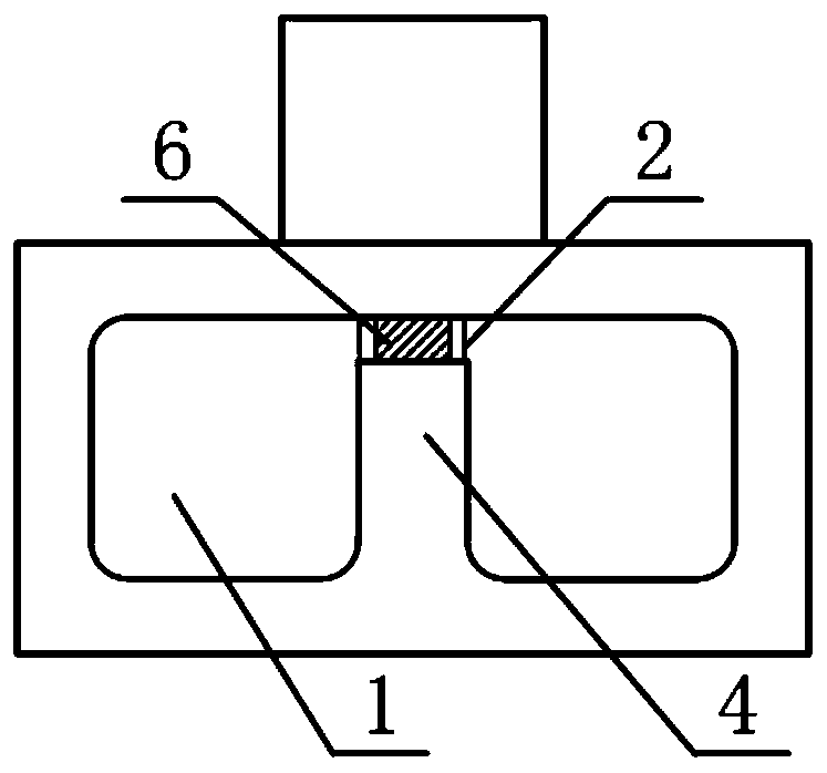
[0017] refer to Figure 1 to Figure 5 . In the preferred embodiment described below, a non-contact ridge waveguide microstrip coupling slot probe transition structure includes: a single ridge waveguide composed of a waveguide ridge back 4 is fabricated in a rectangular waveguide 1, perpendicular to the center of the upper end plane of the rectangular waveguide 1 The windowed waveguide 9 of the line, the waveguide back gap 2 formed by the upper end plane of the waveguide ridge 4 and the upper bottom plane of the rectangular waveguide 1, and the microstrip probe 6 inserted into the window channel of the windowed waveguide 9. It is characterized in that: the waveguide ridge 4 extends below the window at the bottom of the windowed waveguide 9, cuts down and turns vertically to form a section of the ridge open end 3, and is a microstrip substrate inserted downward from the side wall of the window terminal of the windowed waveguide 9 5 is divided into a waveguide coupling slot and ...


PUM


Abstract

The invention discloses a non-contact type ridge waveguide, micro-strip and coupling slot probe transition structure, and aims to provide a transition circuit having wide frequency band and low insertion loss. The non-contact type ridge waveguide, micro-strip and coupling slot probe transition structure in the invention is realized through the following technical scheme: a waveguide ridge extendsto be below the bottom of a windowed waveguide, and forms a section of a ridge open-end after being downwardly cut off and vertically turned; furthermore, it is separated into a waveguide coupling slot and a shielding cavity by a micro-strip substrate, which is downwardly inserted from the side wall of the window terminal of the windowed waveguide; a micro-strip probe is vertically inserted into the coupling slot from the rectangular window of the windowed waveguide; an electromagnetic coupling slot transition area is formed by facing the vertical wall surface of the ridge open-end; an electric field line parallel to the vertical surface of the ridge open-end 3 and an electric field line of the waveguide shielding cavity at the back of the micro-strip substrate act on the surface of the micro-strip probe together, so that surface current is formed; after distributed capacitance between the micro-strip probe and the side wall of the ridge open-end is offset through a section of high-impedance micro-strip line in the window channel of the windowed waveguide, a high-resistance ridge waveguide standard-TE<10> mode is converted into a micro-strip standard-TEM mode; and thus, transitionis completed.

Description

technical field [0001] The invention relates to the field of microwave / millimeter wave circuits, in particular to microwave / millimeter wave modules and components including ridge waveguides, which are mainly used in high-efficiency signal transmission between ridge waveguides and microstrip circuits. Background technique [0002] Although microwave monolithic integrated circuits use microstrip lines to realize signal transmission and interconnection, in many high-power applications, rectangular waveguides are required as the input and output interfaces of radio frequency signals. Therefore, how to design a waveguide-microstrip transition circuit with wide frequency band, low insertion loss, small size and easy fabrication is particularly important, which will have a direct impact on the performance of the system. At present, the commonly used transition conversion methods from waveguide to microstrip include: waveguide-ridge waveguide-microstrip transition, waveguide-couplin...

Claims


Application Information

Patent Timeline
IPC IPC(8): H01P5/107
Inventor 党章朱海帆黄建刘祚麟
Owner 10TH RES INST OF CETC
Why Eureka
Try Eureka