Method for eliminating semiconductor laser COMD and semiconductor laser

A laser and semiconductor technology, applied in the semiconductor field, can solve the problems of high passivation cost and limited improvement of the COMD threshold, and achieve the effect of increasing the surface density of states and improving the COMD threshold.

Inactive Publication Date: 2019-06-21
SUZHOU EVERBRIGHT PHOTONICS
View PDF9 Cites 1 Cited by
  • Summary
  • Abstract
  • Description
  • Claims
  • Application Information

AI Technical Summary

Problems solved by technology

[0003] Therefore, the technical problem to be solved by the present invention is to overcome the disadvantages of limited COMD threshold enhancement and high cost of vacuum cleavage passivation in the prior art, thereby providing a method and device for eliminating COMD of semiconductor lasers

Method used


Image

  • Method for eliminating semiconductor laser COMD and semiconductor laser
  • Method for eliminating semiconductor laser COMD and semiconductor laser
  • Method for eliminating semiconductor laser COMD and semiconductor laser

Examples


Embodiment Construction

[0021] The technical solutions of the present invention will be clearly and completely described below in conjunction with the accompanying drawings. Apparently, the described embodiments are some of the embodiments of the present invention, but not all of them. Based on the embodiments of the present invention, all other embodiments obtained by persons of ordinary skill in the art without making creative efforts belong to the protection scope of the present invention.

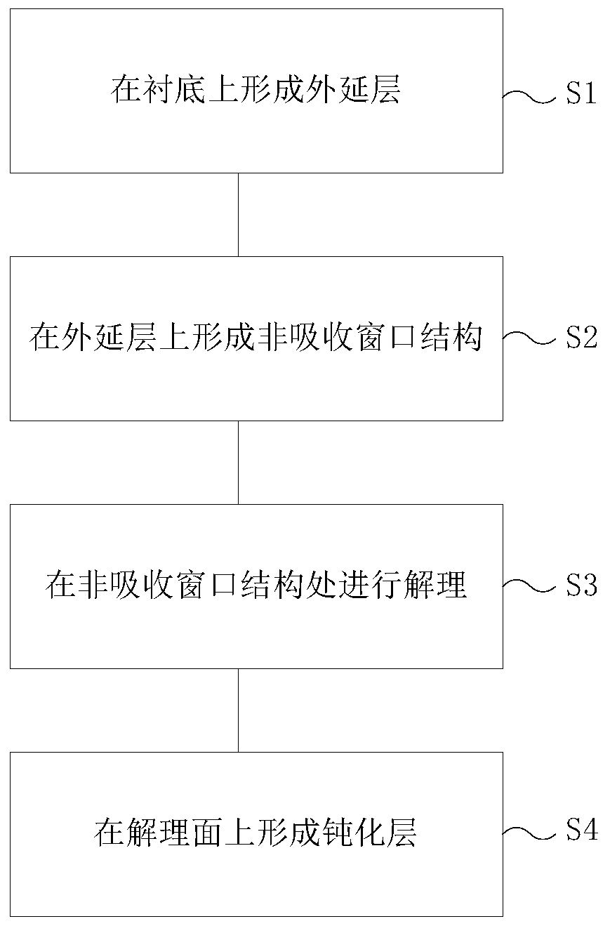
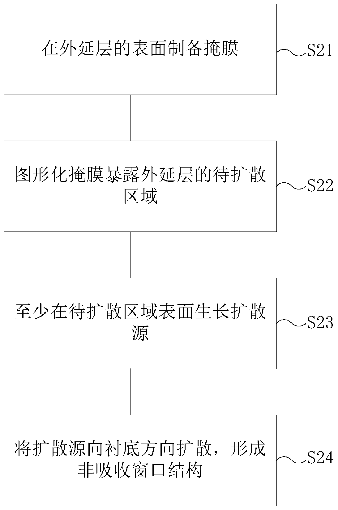
[0022] As mentioned in the background technology, in the prior art, non-absorbing windows are usually made on the epitaxial layer to reduce the absorption of photons, or high-vacuum cleavage passivation is used to reduce the pollution of impurities such as oxygen and carbon on the optical cavity surface. When the laser wavelength is longer, for example, the wavelength above 900nm, the COMD threshold can be improved very well. However, when the wavelength is shorter, no matter whether a non-absorbing window stru...


PUM


Abstract

The invention discloses a method for eliminating a semiconductor laser COMD and a semiconductor laser, wherein the method for eliminating the semiconductor laser COMD comprises the following steps: forming an epitaxial layer on a substrate; forming a non-absorption window structure on the epitaxial layer; cleaving at the non-absorbing window structure; and forming a passivation layer on the cleavage plane. By adopting the method for eliminating the semiconductor laser COMD disclosed by the invention, the forbidden bandwidth of the non-absorption window structure is large, and photons cannot beabsorbed; and since the non-absorption window structure is passivated by vacuum cleavage coating, the surface state density of the non-absorption window structure is low, and the non-radiative recombination of carriers is effectively inhibited, so that the heat productivity of the cavity surface position is extremely low, and the COMD is completely eliminated. Moreover, when the non-absorption window structure is subjected to vacuum cleavage passivation, even if the vacuum degree is reduced moderately, the non-radiative recombination at the cavity surface position can still be ignored in theworking state of the laser, and the COMD threshold value of the laser is not influenced.

Description

technical field [0001] The invention relates to the technical field of semiconductors, in particular to a method for eliminating the COMD of a semiconductor laser and the semiconductor laser. Background technique [0002] Improving the optical output power, lifetime and reliability has always been the focus of research in the field of semiconductor lasers. Catastrophic Optical Mirror Degradation (COMD) is an important factor affecting the optical output power and reliability of semiconductor lasers. COMD is a kind of catastrophic damage caused by the melting of the cavity surface after the laser cavity surface area absorbs the higher optical radiation inside the resonator, causing the temperature to exceed its melting point. In order to solve this problem, the existing technology usually adopts two methods: 1. Vacuum cleavage coating technology, which completes the cleavage and coating process of epitaxial wafers in a high vacuum environment, preventing impurities such as ox...

Claims


Application Information

Patent Timeline
IPC IPC(8): H01S5/02H01S5/028
Inventor 王俊李波程洋胡燚文
Owner SUZHOU EVERBRIGHT PHOTONICS
Why Eureka
Try Eureka