Array substrate, preparation method thereof and display device

A technology of array substrates and substrate substrates, applied in semiconductor/solid-state device manufacturing, electrical components, electric solid-state devices, etc., can solve problems such as increased production costs and expensive masks, and achieves reductions in process preparation costs and savings in masks. Stencil effect

Active Publication Date: 2019-06-25
BOE TECH GRP CO LTD +1
View PDF4 Cites 7 Cited by
  • Summary
  • Abstract
  • Description
  • Claims
  • Application Information

AI Technical Summary

Problems solved by technology

However, masks are more expensive, leading to increased production costs

Method used


Image

  • Array substrate, preparation method thereof and display device
  • Array substrate, preparation method thereof and display device
  • Array substrate, preparation method thereof and display device

Examples


preparation example Construction

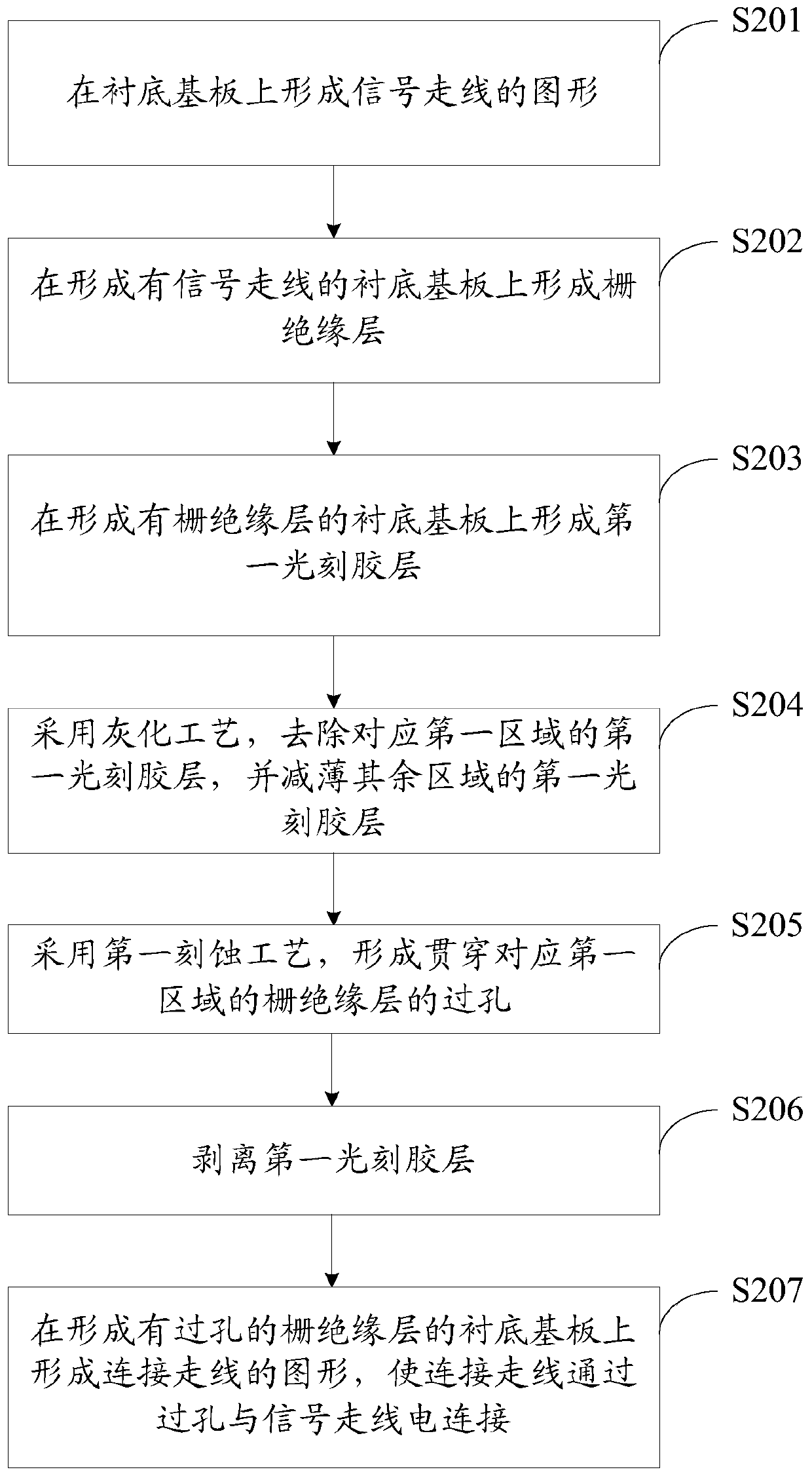
[0051] Based on this, an embodiment of the present invention provides a method for preparing an array substrate, such as figure 2 As shown, the following steps may be included:

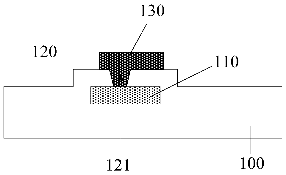
[0052] S201. Form a pattern of signal traces on the base substrate; wherein, in a direction perpendicular to the extension direction of the signal traces, the cross section of the signal traces has a first area and a second area, and on a plane perpendicular to the base substrate, The thickness of the first region is greater than the thickness of the second region. Further, during specific implementation, the first area may be the central area of ​​the signal routing, and the second area may be the edge area of ​​the signal routing;

[0053] S202, forming a gate insulating layer on the substrate on which the signal traces are formed;

[0054] S203, forming a first photoresist layer on the base substrate on which the gate insulating layer is formed; wherein, the thickness of the first photoresist laye...


PUM


Abstract

The invention discloses an array substrate, a preparation method thereof, and a display device. The thickness of a first region of a cross section, perpendicular to an extending direction of a signalline, of the signal line is greater than the thickness of a second region, so after a gate insulating layer and a first photoresist layer are formed, the thickness of the first photoresist layer corresponding to the first region can be less than the thickness of the other regions because the material of the first photoresist layer has flowability. In this way, the first photoresist layer is processed through the ashing technology, the first photoresist layer corresponding to the first area is removed and only the first photoresist layer in the rest areas is thinned, so that the gate insulatinglayer corresponding to the first area is directly exposed, and a via hole is formed through the etching technology. Therefore, the first photoresist layer above the first region corresponding to thesignal line can be removed without a mask plate, so that the gate insulating layer forms a via hole, thereby saving a mask plate, and reducing the process preparation cost.

Description

technical field [0001] The present invention relates to the field of display technology, in particular to an array substrate, a preparation method thereof and a display device. Background technique [0002] Generally, a mask plate is required in the manufacturing process of the array substrate in the display panel. Since array substrates with different structures correspond to different mask structures, it is necessary to prepare a plurality of mask plates with different structures to meet the requirements for preparing array substrates with different structures. However, the mask plate is more expensive, resulting in increased production costs. Contents of the invention [0003] Embodiments of the present invention provide an array substrate, a manufacturing method thereof, and a display device, so as to reduce production costs. [0004] An embodiment of the present invention provides a method for preparing an array substrate, including: [0005] A pattern of signal tr...

Claims


Application Information

Patent Timeline
Patent Type & Authority Applications(China)
IPC IPC(8): H01L21/027H01L21/84H01L27/12
CPCH01L21/027H01L21/84H01L27/12
Inventor 宁智勇周宏儒田茂坤王恺谌伟豆远尧王思江黄中浩
Owner BOE TECH GRP CO LTD
Why Eureka
Try Eureka