Mass Micro LED transfer method and mass transfer device

A technology of transfer method and transfer device, which is applied in semiconductor/solid-state device testing/measurement, electrical components, electric solid-state devices, etc., and can solve problems that need to be improved

Inactive Publication Date: 2019-06-28
HEFEI XINSHENG OPTOELECTRONICS TECH CO LTD +1
View PDF5 Cites 32 Cited by
  • Summary
  • Abstract
  • Description
  • Claims
  • Application Information

AI Technical Summary

Problems solved by technology

[0004] Therefore, the current mass transfer tec

Method used


Image

  • Mass Micro LED transfer method and mass transfer device
  • Mass Micro LED transfer method and mass transfer device
  • Mass Micro LED transfer method and mass transfer device

Examples


Embodiment Construction

[0046] The following describes the embodiments of the present invention in detail, and those skilled in the art will understand that the following embodiments are intended to explain the present invention, and should not be regarded as limiting the present invention. Unless otherwise specified, in the following examples that do not explicitly describe specific techniques or conditions, those skilled in the art can carry out according to commonly used techniques or conditions in this field or according to product instructions.

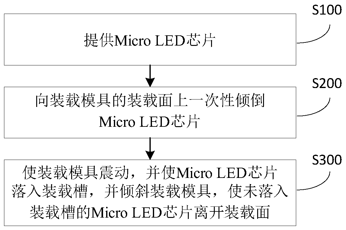
[0047] In one aspect of the present invention, the present invention proposes a method for mass transfer of Micro LEDs. According to an embodiment of the present invention, refer to figure 1 , the mass transfer methods include:

[0048] S100: Provide Micro LED chips.

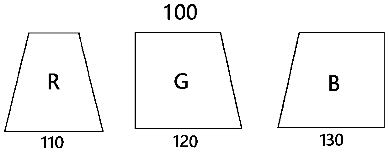
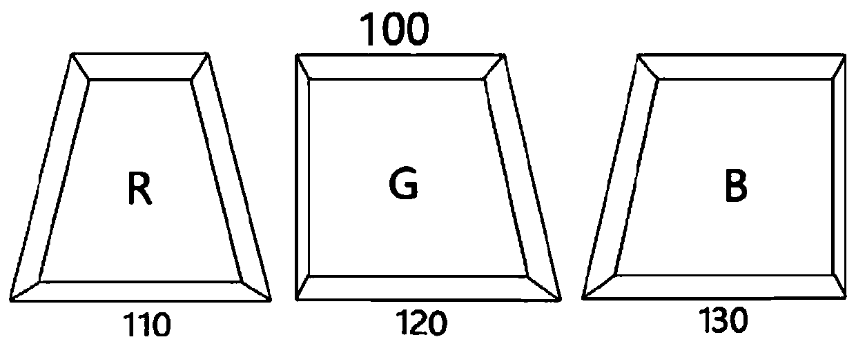
[0049] In this step, Micro LED chips 100 of multiple colors are provided, and the cross-sectional shape of the Micro LED chip 110 capable of emitting a first color is different from the...


PUM

PropertyMeasurementUnit
Angleaaaaaaaaaa
Depthaaaaaaaaaa

Abstract

The invention proposes a mass Micro LED transfer method and a mass transfer device. The method comprises a step of providing Micro LED chips, wherein the cross-sectional shapes of first Micro LED chips capable of emitting a first color is different from the cross-sectional shapes of second Micro LED chips capable of emitting a second color, a step of dumping the Micro LED chips on a loading surface of a loading mold at one time, wherein the loading surface is provided with loading slots with first shapes matched with the shapes of the first Micro LED chips and second shapes matched with the shapes of the second Micro LED chips, and a step of vibrating the loading mold and allowing the Micro LED chips to fall into the matched loading slots, and tilting the loading mold such that Micro LED chips that do not fall into the loading slots leave the loading surface. The mass transfer method proposed by the invention can realize the mass transfer process of a plurality of Micro LED chips withdifferent colors at one time, and the high transfer yield can be ensured while the transfer efficiency is multiplied.

Description

technical field [0001] The present invention relates to the technical field of Micro LED manufacturing, and in particular, the present invention relates to a mass transfer method and a mass transfer device for Micro LEDs. Background technique [0002] Compared with traditional liquid crystal display panels, micro light-emitting diode (Micro LED) display panels have advantages such as higher resolution, better contrast ratio, faster response time and lower energy consumption, so they are regarded as the next-generation display technology. After the Micro LED chip is manufactured, tens of thousands to hundreds of thousands of Micro LED chips need to be transferred to the driving circuit board to form an LED array. This process is called "mass transfer". Due to the small size of Micro LED, while ensuring the efficiency and yield of transfer, it has become a major problem in the process of Micro LED industrialization. [0003] At the present stage, the mass transfer process of ...

Claims


Application Information

Patent Timeline
IPC IPC(8): H01L21/67H01L27/15
CPCH01L21/67H01L22/22H01L25/0753H01L33/0095H01L21/6835H01L2221/68322H01L2221/68354H01L2221/68313H01L33/20H01L22/20H01L33/62H01L2221/68368H01L2933/0066
Inventor 王国华
Owner HEFEI XINSHENG OPTOELECTRONICS TECH CO LTD
Why Eureka
Try Eureka