Split gate type memory and formation method thereof

A split-gate memory, floating gate technology, applied in the direction of electric solid devices, semiconductor devices, electrical components, etc., can solve the problems of wafer size reduction, coupling area influence, etc., to reduce the coupling coefficient, reduce the erasing voltage, The effect of increasing the coupling area

Active Publication Date: 2019-06-28
SHANGHAI HUAHONG GRACE SEMICON MFG CORP
View PDF6 Cites 0 Cited by
  • Summary
  • Abstract
  • Description
  • Claims
  • Application Information

AI Technical Summary

Problems solved by technology

[0002] In existing split-gate memories, such as figure 1 As shown, the floating gate FG is partly located above the source region SL and is insulated from it, wherein the overlapping portion of the source region SL and the floating gate FG accounts for about 1 / 2 of the length of the floating gate FG, which is used for source region SL during programming. The pole-to-floating gate FG coupling generates high voltage, which attracts electrons to tunnel to the floating gate FG, but the longer coupling area affects the reduction of wafer size

Method used


Image

  • Split gate type memory and formation method thereof
  • Split gate type memory and formation method thereof
  • Split gate type memory and formation method thereof

Examples


Embodiment Construction

[0055] In order to describe the technical solution of the above invention in more detail, specific examples are listed below to demonstrate the technical effect; it should be emphasized that these examples are used to illustrate the present invention and not limit the scope of the present invention.

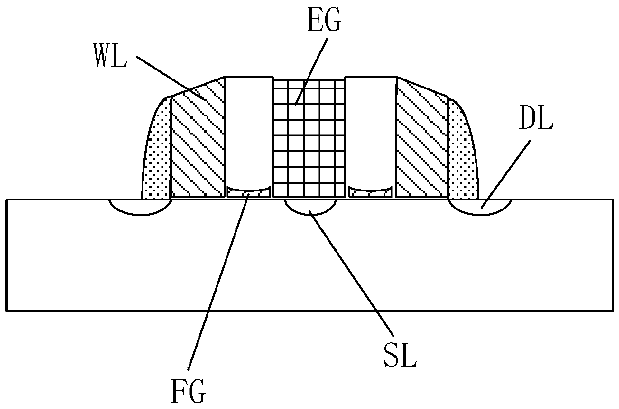
[0056] For the split-gate memory provided by the present invention, please refer to Figure 2s ,include:

[0057] A substrate 100, on which a source region SL and a drain region DL are formed, and a source line 200 contacting and conducting with the source region SL is arranged above the source region SL, as extension of the source;

[0058] an erase gate 400 disposed above the source line 200; and

[0059] The floating gate FG and the word line WL are laterally adjacently arranged on the substrate 100 between the source region SL and the drain region DL, wherein the floating gate FG is close to the source line 200, so The word line WL is far away from the source line 200;

...


PUM


Abstract

The invention relates to a split gate type memory and a formation method thereof The split gate type memory comprises a substrate, an erasing gate, a floating gate, a word line and insulating layers;source and drain areas are formed on the substrate, and a source line in contact connection with the source area is formed on the source area; the erasing gate is arranged on the source line; the floating gate and word line are arranged horizontally adjacent to each other on the substrate between the source and drain areas, the floating gate is close to the source line, and the word line is far from the source line; and the insulating layers are formed between the source line, erasing gate, floating gate and word line. The source line higher than the upper surface of the substrate is arranged,so that the floating gate and the source area form an overlapped area in the vertical direction, and the height of the source line is adjustable, so that a coupling efficiency between the floating gate and the source area is ensured while the wafer size is reduced.

Description

technical field [0001] The invention relates to the technical field of semiconductor manufacturing, in particular to a split-gate memory and a forming method thereof. Background technique [0002] In existing split-gate memories, such as figure 1 As shown, the floating gate FG is partly located above the source region SL and is insulated from it, wherein the overlapping portion of the source region SL and the floating gate FG accounts for about 1 / 2 of the length of the floating gate FG, which is used for source region SL during programming. The coupling of the electrode to the floating gate FG generates a high voltage, which attracts electrons to tunnel to the floating gate FG, but the longer coupling area affects the reduction of the wafer size. [0003] Therefore, how to provide a split-gate memory and its forming method that can reduce the length of the floating gate FG on the plane under the premise of ensuring the coupling coefficient of the source to the floating gate...

Claims


Application Information

Patent Timeline
Patent Type & Authority Applications(China)
IPC IPC(8): H01L27/11521
Inventor 于涛
Owner SHANGHAI HUAHONG GRACE SEMICON MFG CORP
Why Eureka
Try Eureka