
High voltage half bridge drive circuit

A high-voltage drive circuit and high-side drive technology, which is applied in the direction of electronic switches, electrical components, output power conversion devices, etc., can solve the problem of low switching efficiency of half-bridge circuits, insufficient gate-source voltage difference, and inability to conduct MOS tubes, etc. problem, to achieve the effect of small on-resistance

Active Publication Date: 2020-09-22
NORTHWESTERN POLYTECHNICAL UNIV
View PDF4 Cites 0 Cited by
  • Summary
  • Abstract
  • Description
  • Claims
  • Application Information

AI Technical Summary

Problems solved by technology

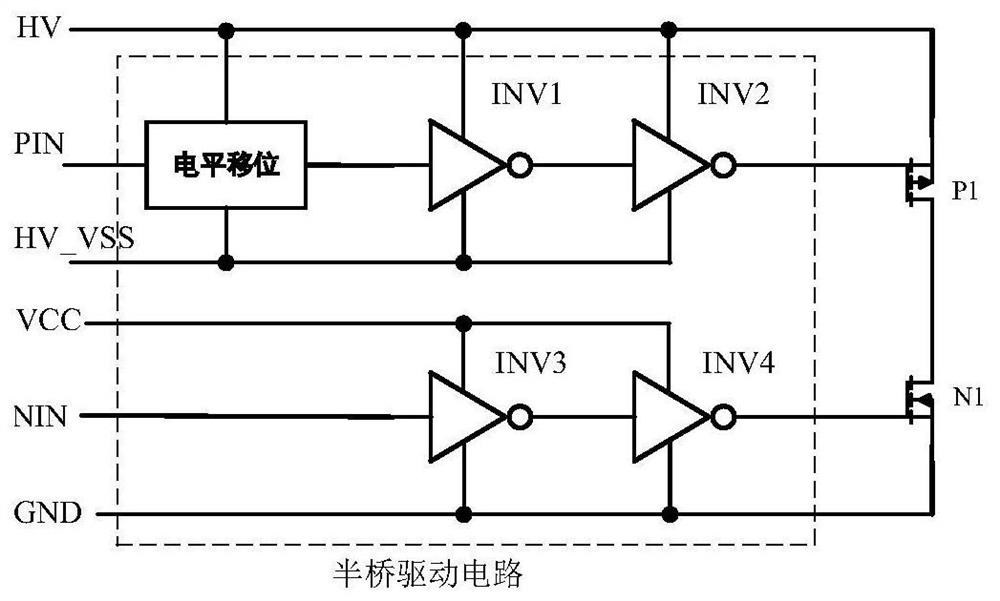
Therefore, the gate-source driving voltage of the half-bridge MOS transistors P1 and N1 is also less than 5.5V. Obviously, the gate-source voltage difference is not enough to fully conduct the MOS transistors, making the switching efficiency of the half-bridge circuit low.

Method used


Image

  • High voltage half bridge drive circuit
  • High voltage half bridge drive circuit
  • High voltage half bridge drive circuit

Examples


Embodiment Construction

[0018] Now in conjunction with embodiment, accompanying drawing, the present invention will be further described:

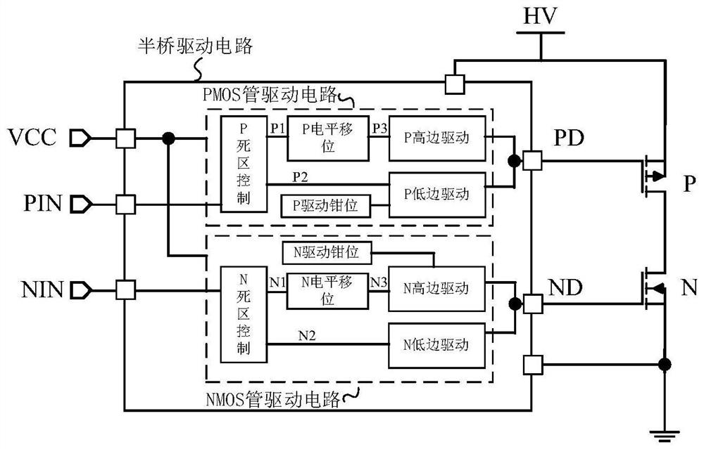
[0019] The working principle of the present invention is: the overall block diagram of the high-voltage half-bridge driving circuit described in the present invention is as follows figure 2 , the drains of the PMOS power transistor P and the NMOS power transistor N are connected, the source of the PMOS power transistor is connected to the high-voltage power supply HV, the source of the NMOS power transistor is grounded to GND, and the PMOS power transistor P and the NMOS power transistor N form a half-bridge structure. Wherein the logic signal PIN controls the gate PD terminal of the PMOS power transistor P through the high-voltage half-bridge driving circuit described in the present invention, thereby controlling the opening and closing of P, and at the same time, the logic signal NIN passes through the high-voltage half-bridge driving circuit described in the p...


PUM


Abstract

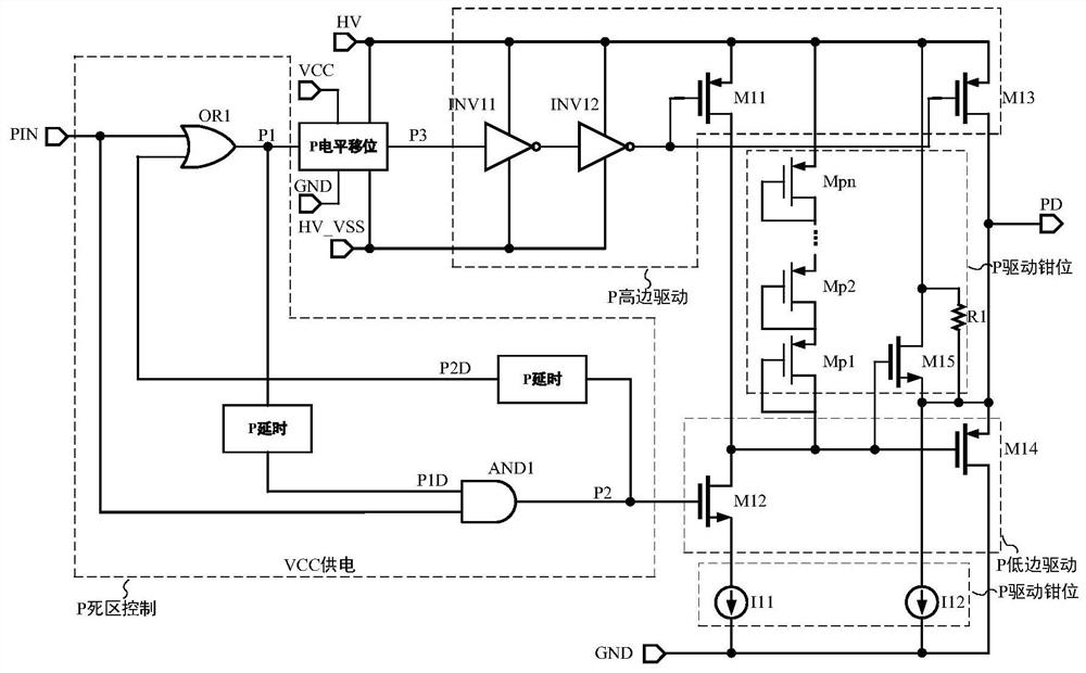
The invention relates to a high-voltage half-bridge driving circuit, and the circuit comprises a PMOS high-voltage driving circuit and an NMOS high-voltage driving circuit, which are respectively usedfor driving a PMOS power tube and an NMOS power tube. The PMOS high-voltage driving circuit comprises a P dead zone control circuit, a P level shift circuit, a P driving clamping circuit, a P high-side driving circuit and a P low-side driving circuit. A driving signal PIN of the PMOS transistor P is connected with the P dead zone control circuit, and the P dead zone control circuit is connected with the P level shift circuit and the P low-side driving circuit; the P driving clamping circuit is connected with the P low-side driving circuit, and the P level shift circuit is connected with the Phigh-side driving circuit; the output of the P high-side driving circuit and the output of the P low-side driving circuit are connected to form a PD, and the PD is connected with the grid electrode of a PMOS power tube in the half-bridge structure to drive the power tube P to be turned on and off; and the NMOS high-voltage driving circuit is similar to the PMOS high-voltage driving circuit. The half-bridge PMOS transistor and the half-bridge NMOS transistor can be provided for providing high-voltage gate source driving, thereby reducing the conduction impedance of the half-bridge MOS transistor.

Description

technical field [0001] The invention belongs to the technical field of power management, and relates to an analog integrated circuit, in particular to a high-voltage half-bridge drive circuit. Background technique [0002] Half-bridge circuits composed of PMOS transistors and NMOS transistors are widely used. For example, half-bridge circuits are indispensable in DC-DC, AC-DC, and DC-AC conversion circuits. As the power and working voltage of power tubes gradually increase, for driving high-power MOS tubes working in high-voltage regions, and increasing the gate-source voltage to reduce the on-resistance of MOS tubes, low power consumption, etc., the need for external discrete components The drive circuit design of high-voltage and high-power MOS tubes puts forward higher requirements. [0003] Traditional high-voltage drive circuit structure such as figure 1 , use the inverter to directly drive the half-bridge PMOS and NMOS tubes. The NMOS driving logic input NIN is conn...

Claims


Application Information

Patent Timeline
Patent Type & Authority Patents(China)
IPC IPC(8): H02M1/088H03K17/687
Inventor 刘雨鑫张豪郑怀仓
Owner NORTHWESTERN POLYTECHNICAL UNIV
Learn More