Structural design of high-power planar gate D-MOSFET
A structural design, planar gate technology, applied in electrical components, circuits, semiconductor devices, etc., can solve problems such as reducing the maximum electric field strength, reduce the maximum electric field strength, improve the wafer utilization rate, increase the available on-current density and Effects of inrush current performance
- Summary
- Abstract
- Description
- Claims
- Application Information
AI Technical Summary
Problems solved by technology
Method used
Image
Examples
Embodiment 1
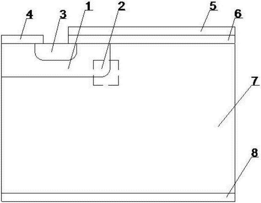
[0033] Such as figure 1 Shown is the D-MOSFET structure in the prior art. In this example, figure 1 The planar gate D-MOSFET shown is N-MOS structure, in which 1-P-well, 2-P-well corner region, 3-N+ source region, 4-source level, 5-gate level, 6-insulation layer, 7 -N-drift region, 8-drain stage. When D-MOSFET devices are blocking high voltage, such as figure 1 The P-N junction formed by the shown N-drift region / P-well is reverse biased, and a very high-intensity electric field is generated near the N-drift region / P-well interface. This electric field increases in the area where the curvature of the P-N junction interface is large, and the maximum intensity electric field appears in the P-well corner region 2 of the N-drift region / P-well interface in the D-MOSFET.
[0034] In the widely used wide bandgap material D-MOSFET design at present, the P-well 1 region is implanted with ions through a single mask. Due to the limited diffusion rate of the dopant atoms used in the w...
Embodiment 2
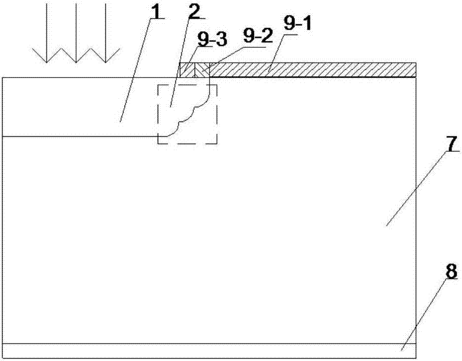
[0047] Such as Figure 4 Shown is a schematic diagram of the structural design of a high-power planar gate D-MOSFET. The corner area is a ladder structure composed of three arcs, but the angle 10 of each batch of ion implantation can be adjusted to produce small sub-steps with different corner curvatures. Each sub-step can use its own independent corner curvature. A small sub-step with a smaller curvature or a larger corner radius can be placed in the deepest part of the P-well as the first corner to further reduce the maximum electric field intensity at the P-well / N-drift region interface, as shown in the figure The radian radius of the bottom sub-step is 1.5 times that of the remaining two steps.
[0048] In a modified embodiment of this embodiment, the arc radius of the lowest sub-step may be any multiple of the remaining steps.
Embodiment 3
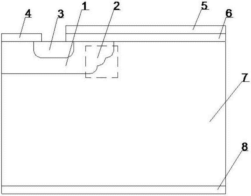
[0050] Such as Figure 5 Shown is a schematic diagram of the structural design of the high-power planar gate D-MOSFET. Small sub-steps with different spatial distribution can be produced by adjusting the basic energy of each ion implantation batch, the angle 10 during ion implantation, and the width of the ion implantation window of the corresponding mask, that is, each sub-step can use its own independent depth and width. figure 2 Shown is a linear spatial distribution, non-linear distributions, such as arc-shaped distributions, can be produced by the aforementioned methods. Such as Figure 5 As shown, there is an incremental area generated by a circular arc distribution in the step of the corner area, and the hatched area is the incremental groove grid area formed after the convex circular arc distribution is formed. The curvature of the equivalent P-well / N-drift region interface can be reduced by adopting a circular arc or curved distribution, thereby reducing the maxim...
PUM
 Abstract
Description
Claims
Application Information


