Fingerprint identification module and fingerprint identification equipment

A fingerprint identification module and fingerprint identification technology, which is applied in the direction of acquiring/arranging fingerprints/palmprints, character and pattern recognition, instruments, etc., can solve the problem of difficult process of fingerprint identification module, complex film structure of fingerprint identification module, Issues such as the limitation of the size of the fingerprint sensor electrode space, to achieve the effect of reducing thickness, reducing process difficulty, and improving light stability

Pending Publication Date: 2019-07-12
GUANG ZHOU NEW VISION OPTO ELECTRONICS TECH
View PDF0 Cites 8 Cited by
  • Summary
  • Abstract
  • Description
  • Claims
  • Application Information

AI Technical Summary

Problems solved by technology

[0005] In view of this, the object of the present invention is to propose a fingerprint recognition module and a fingerprint recognition device to solve the problem that the fingerprint sensing electrode is limited by the size of the space, the film layer structure of the fingerprint recognition module is relatively complicated, and the process of preparing the fingerprint recognition module more difficult questions

Method used


Image

  • Fingerprint identification module and fingerprint identification equipment
  • Fingerprint identification module and fingerprint identification equipment
  • Fingerprint identification module and fingerprint identification equipment

Examples


Embodiment Construction

[0033] The technical solutions of the present invention will be further described below in conjunction with the accompanying drawings and through specific implementation methods. It should be understood that the specific embodiments described here are only used to explain the present invention, but not to limit the present invention. In addition, it should be noted that, for the convenience of description, only some structures related to the present invention are shown in the drawings but not all structures.

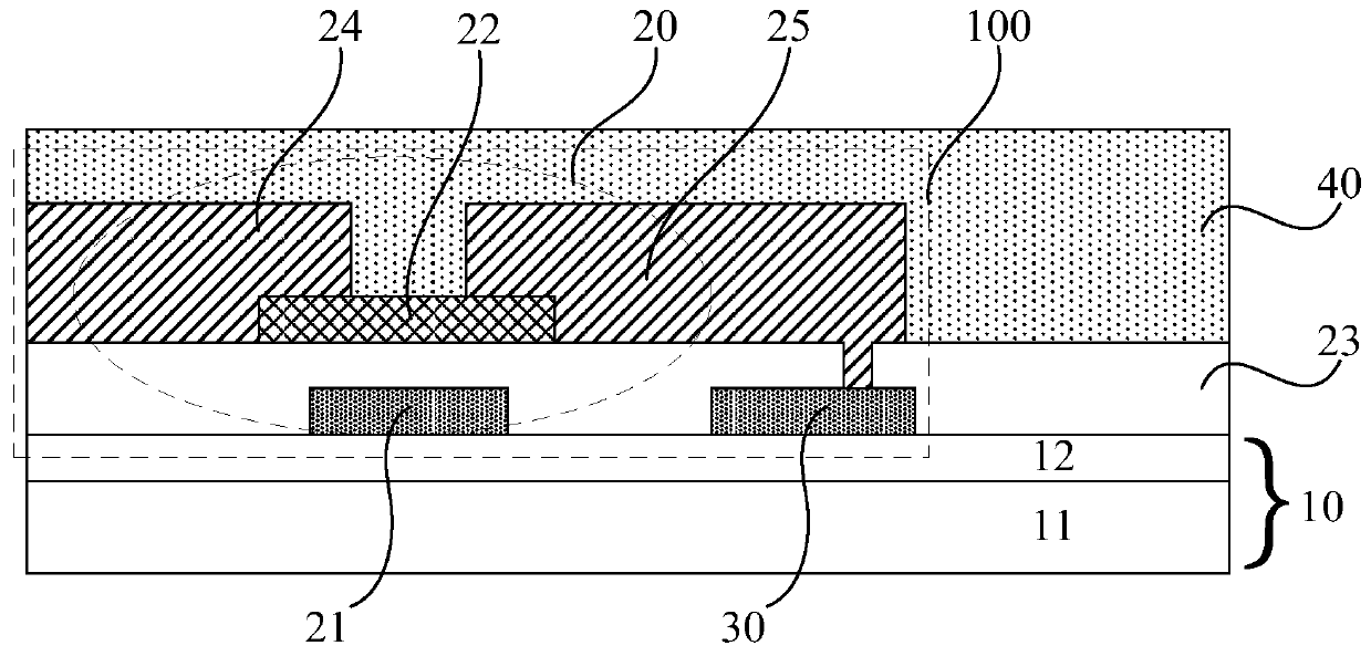
[0034] figure 1 It is a schematic structural diagram of a fingerprint recognition module provided by an embodiment of the present invention, which can be applied to a fingerprint recognition device with a fingerprint recognition function, and can realize thinning of the fingerprint recognition device. Such as figure 1 As shown, the fingerprint identification module provided in this embodiment includes:

[0035] transparent substrate 10;

[0036] At least one fingerpr...


PUM


Abstract

The invention discloses a fingerprint identification module and fingerprint identification equipment. The fingerprint identification module comprises: a transparent substrate; at least one fingerprintidentification unit which is located on one side of the transparent substrate, wherein the sensing surface of the fingerprint identification unit is arranged towards the transparent substrate, the fingerprint identification unit comprises a thin film transistor and a fingerprint sensing electrode, the thin film transistor comprises a grid electrode, a metal oxide semiconductor thin film doped with rare earth oxide and a grid insulating layer located between the grid electrode and the metal oxide semiconductor thin film, and a source electrode and a drain electrode which are respectively connected with the metal oxide semiconductor film; the source electrode or the drain electrode is electrically connected with the fingerprint sensing electrode, and the fingerprint sensing electrode, the grid electrode, the source electrode and the drain electrode are all transparent electrodes. The problems that a fingerprint sensing electrode is limited by the space size, the film layer structure ofthe fingerprint recognition module is complex, and the process difficulty of preparing the fingerprint recognition module is large are solved.

Description

technical field [0001] The embodiment of the present invention relates to the technical field of fingerprint identification, in particular to a fingerprint identification module and a fingerprint identification device. Background technique [0002] With the rapid development of display technology, display panels with a fingerprint identification function have gradually become popular. [0003] Existing fingerprint identification units usually include thin film transistors and fingerprint sensing electrodes. Since electrodes in existing thin film transistors and fingerprint sensing electrodes are generally metal electrodes, in order to avoid reducing the aperture ratio of the display panel, the fingerprint identification unit needs to be arranged on The gap area between the pixel units limits the position of the fingerprint identification unit, which increases the difficulty of the process; and the area of ​​the gap area is very small, and the fingerprint sensing electrode ca...

Claims


Application Information

Patent Timeline
Patent Type & Authority Applications(China)
IPC IPC(8): G06K9/00
CPCG06V40/1318
Inventor 陶洪周雷徐苗李洪濛陈禧张琪
Owner GUANG ZHOU NEW VISION OPTO ELECTRONICS TECH
Why Eureka
Try Eureka