

Pixel compensating circuit, driving method thereof, display panel and display device
A technology for compensating circuits and pixels, applied to static indicators, instruments, etc., can solve problems affecting image display effects and uneven display brightness, and achieve the effects of improving uniformity, maintaining stable driving current, and avoiding impact
- Summary
- Abstract
- Description
- Claims
- Application Information
AI Technical Summary
Problems solved by technology
Method used
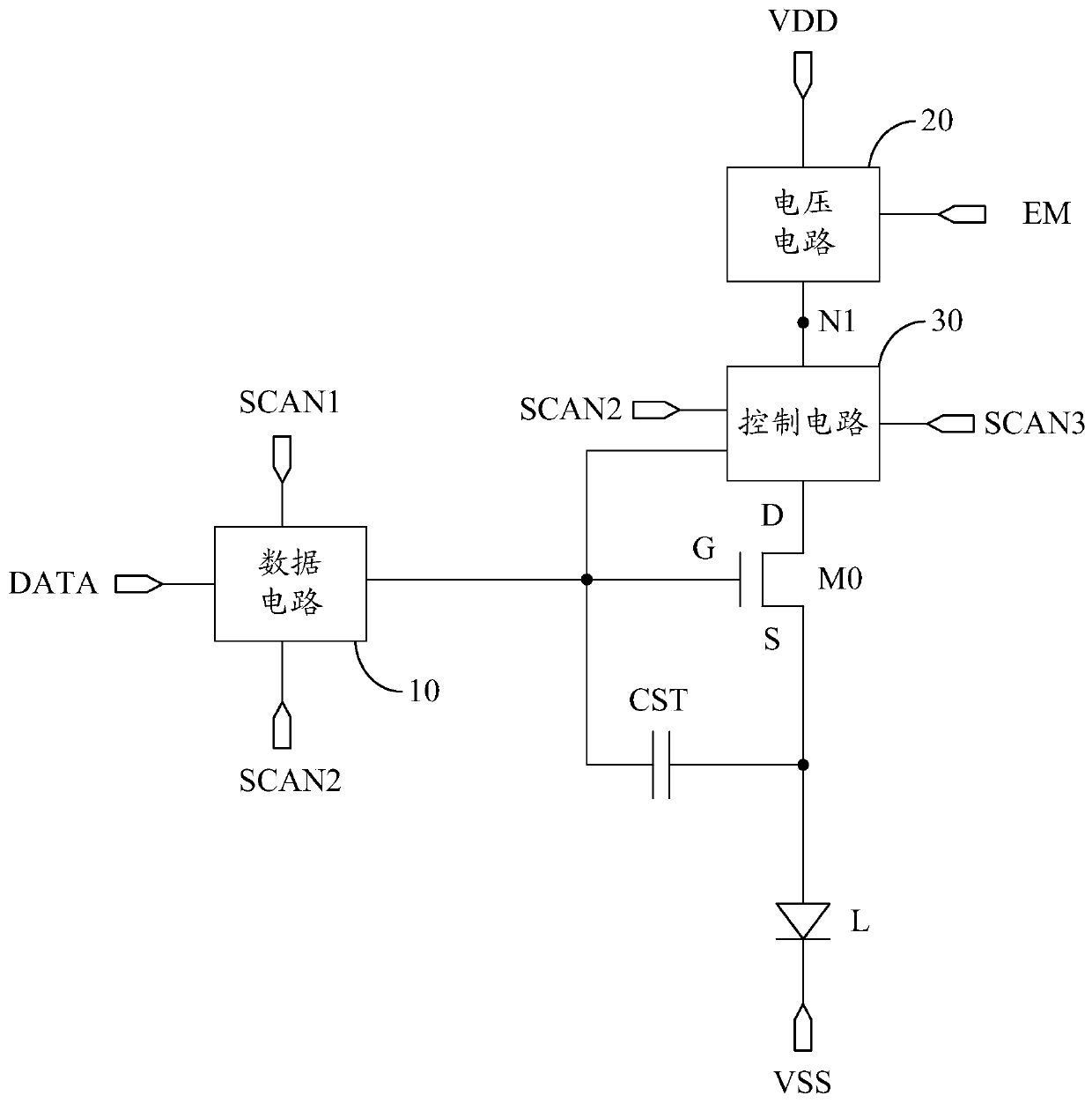
Image

Examples
Embodiment 1
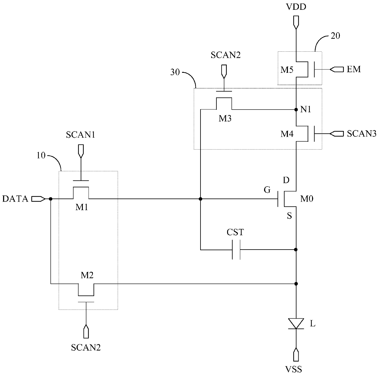
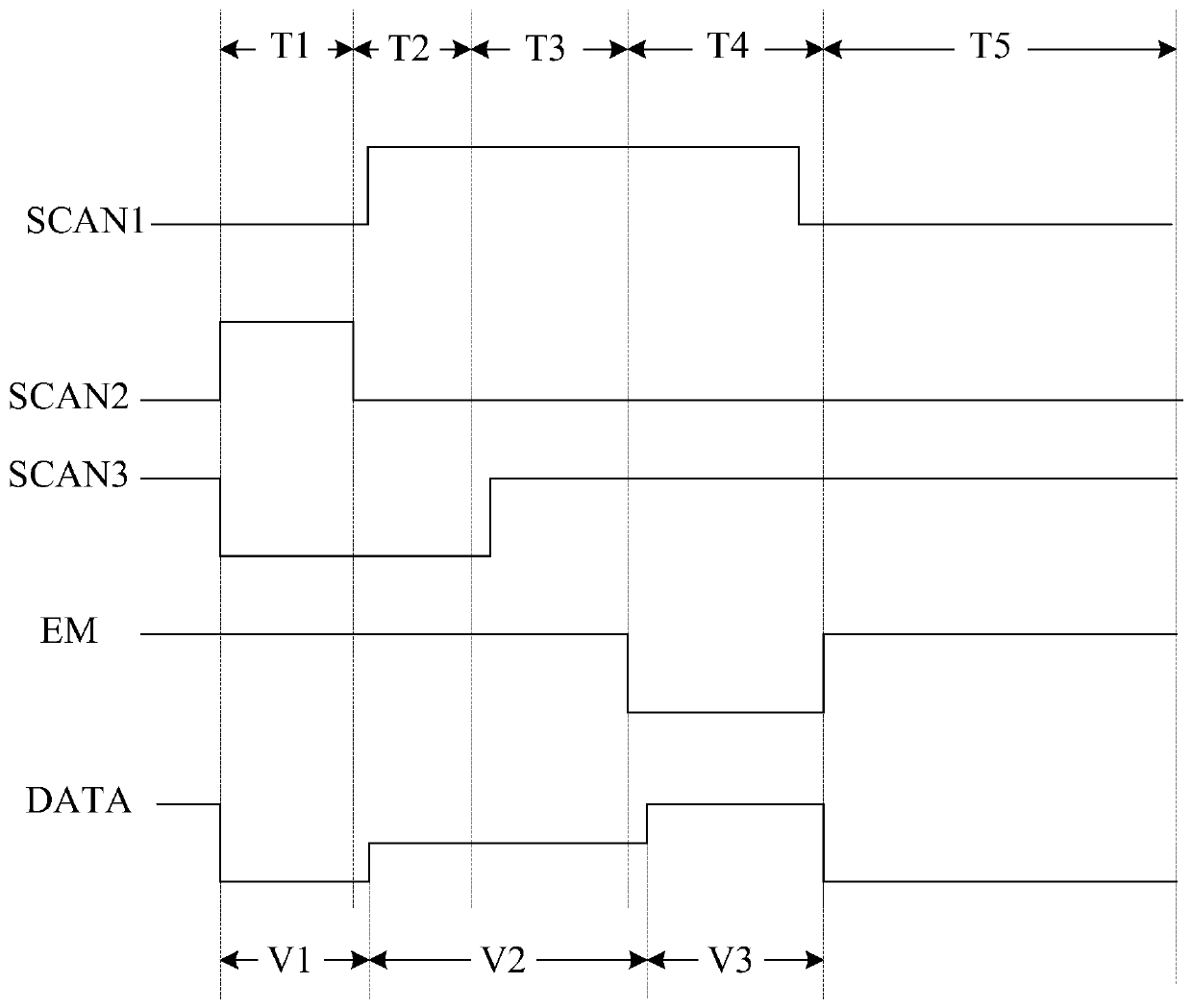
[0070] figure 2 The circuit timing diagram corresponding to the pixel compensation circuit shown in image 3 shown. Specifically, choose the image 3 In the shown input timing diagram, there are five stages in total including recovery stage T1 , voltage adjustment stage T2 , threshold value latch stage T3 , data input stage T4 and light emitting stage T5 .
[0071] In the recovery phase T1, SCAN1=0, SCAN2=1, SCAN3=0, EM=1.
[0072] Since SCAN1=0, the first switching transistor M1 is turned off. Since SCAN3=0, the fourth switching transistor M4 is turned off. Since SCAN2=1, both the second switching transistor M2 and the third switching transistor M3 are turned on. Since EM=1, the fifth switching transistor M5 is turned on. The turned-on fifth switch transistor M5 and the third switch transistor M3 provide the voltage Vdd of the signal of the first voltage signal terminal VDD to the gate of the driving transistor M0, so that the voltage of the gate of the driving transis...
Embodiment 2
[0086] figure 2 The circuit timing diagram corresponding to the pixel compensation circuit shown in Figure 4 shown. Specifically, choose the Figure 4 In the shown input timing diagram, there are five stages in total including recovery stage T1 , voltage adjustment stage T2 , threshold value latch stage T3 , data input stage T4 and light emitting stage T5 .
[0087] In the recovery phase T1, the voltage of the signal at the first voltage signal terminal VDD is the second preset power supply voltage Vdd2, SCAN1=0, SCAN2=1, SCAN3=0, EM=1.
[0088] Since SCAN1=0, the first switching transistor M1 is turned off. Since SCAN3=0, the fourth switching transistor M4 is turned off. Since SCAN2=1, both the second switching transistor M2 and the third switching transistor M3 are turned on. Since EM=1, the fifth switching transistor M5 is turned on. The turned-on fifth switching transistor M5 and the third switching transistor M3 provide the signal of the second preset power supply...
PUM
 Abstract
Description
Claims
Application Information