
Semiconductor device and semiconductor structure

A semiconductor, oxide semiconductor technology, used in semiconductor devices, semiconductor/solid-state device manufacturing, transistors, etc.

Active Publication Date: 2019-07-12
NUVOTON
View PDF5 Cites 0 Cited by
  • Summary
  • Abstract
  • Description
  • Claims
  • Application Information

AI Technical Summary

Problems solved by technology

However, the performance of current high electron mobility transistors needs to be further improved

Method used


Image

  • Semiconductor device and semiconductor structure
  • Semiconductor device and semiconductor structure
  • Semiconductor device and semiconductor structure

Examples


Embodiment Construction

[0047] In order to make the purpose, features and advantages of the present invention more comprehensible, the following specific examples are given together with the accompanying drawings for a detailed description. The description of the present invention provides different examples to illustrate the technical features of different implementations of the present invention. Wherein, the configuration of each element in the embodiment is for illustration, not for limiting the present invention. In addition, part of the symbols in the figures in the embodiments are repeated for the purpose of simplifying the description, and do not imply the relationship between different embodiments.

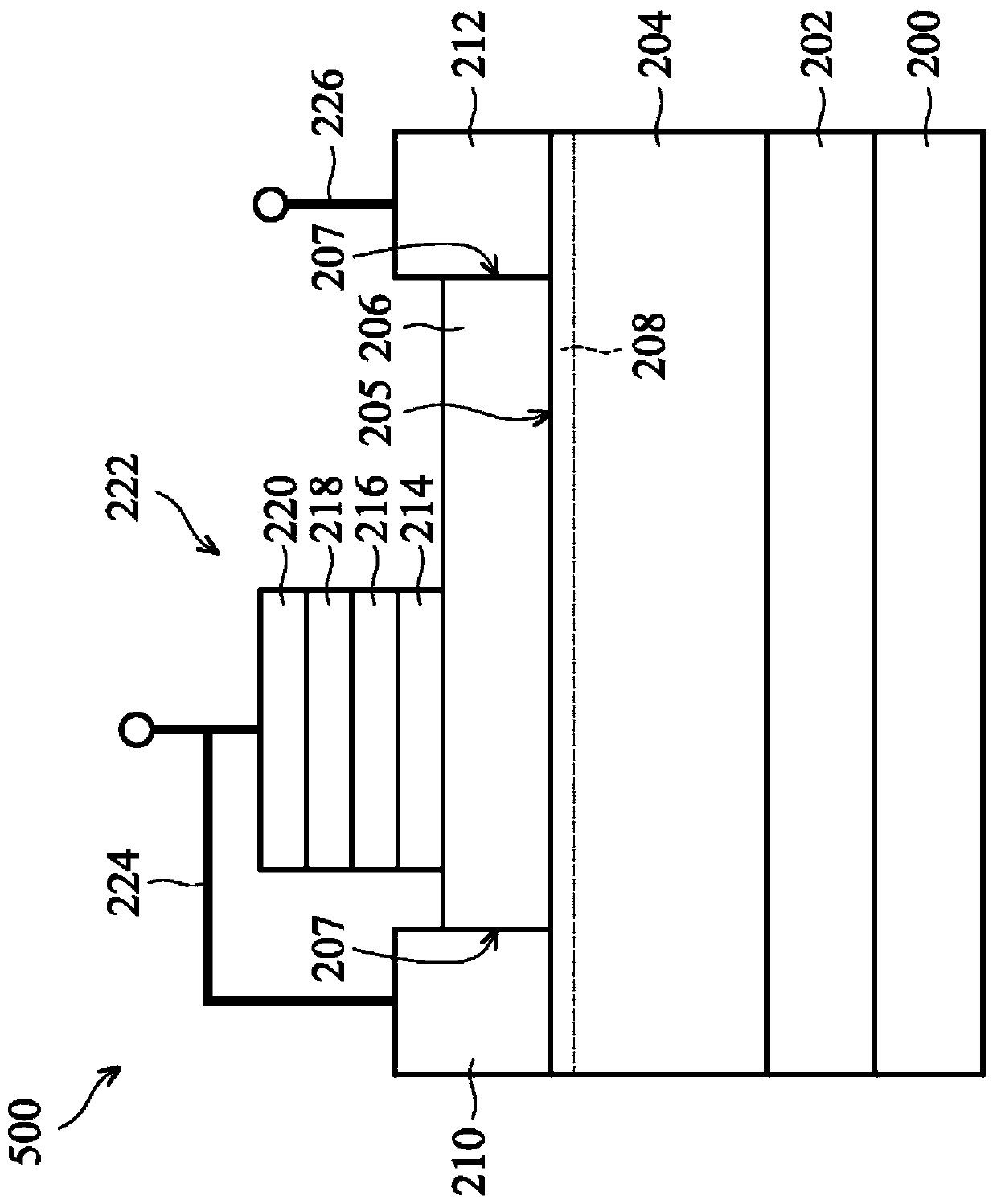
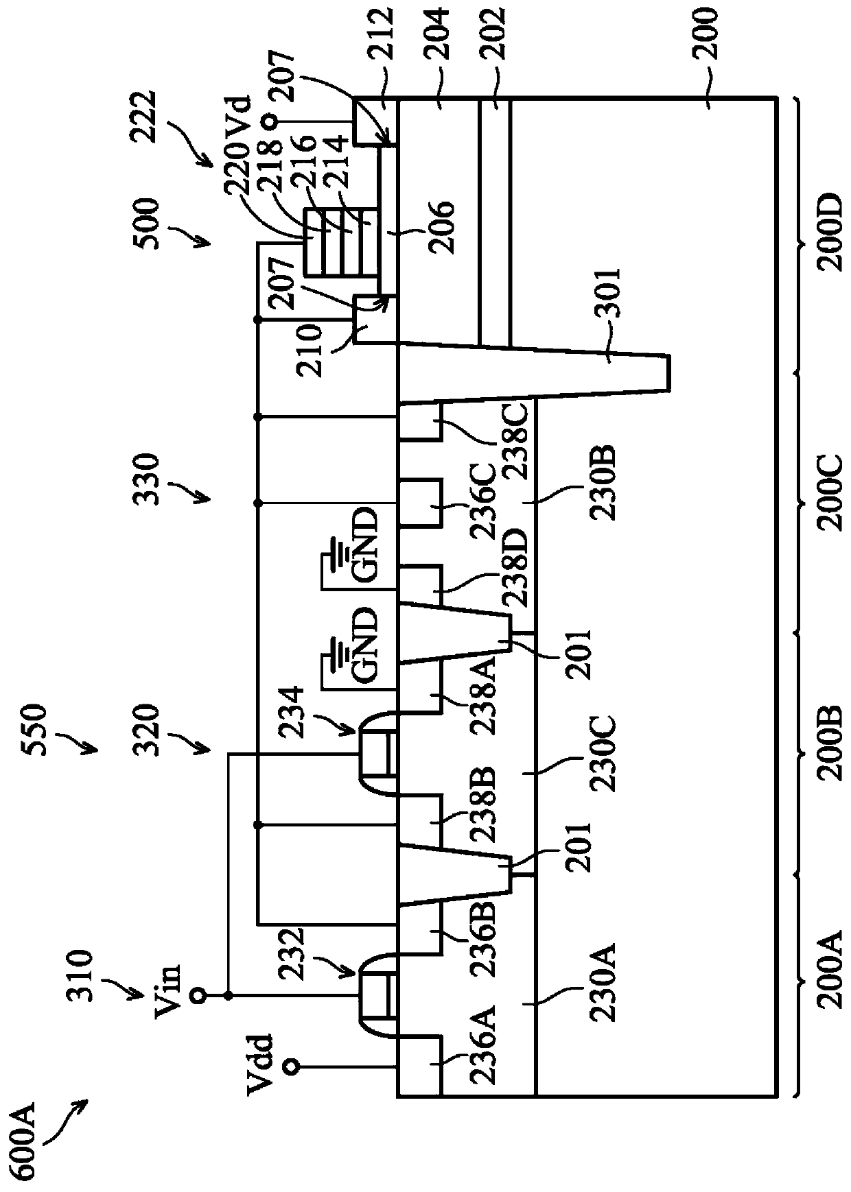
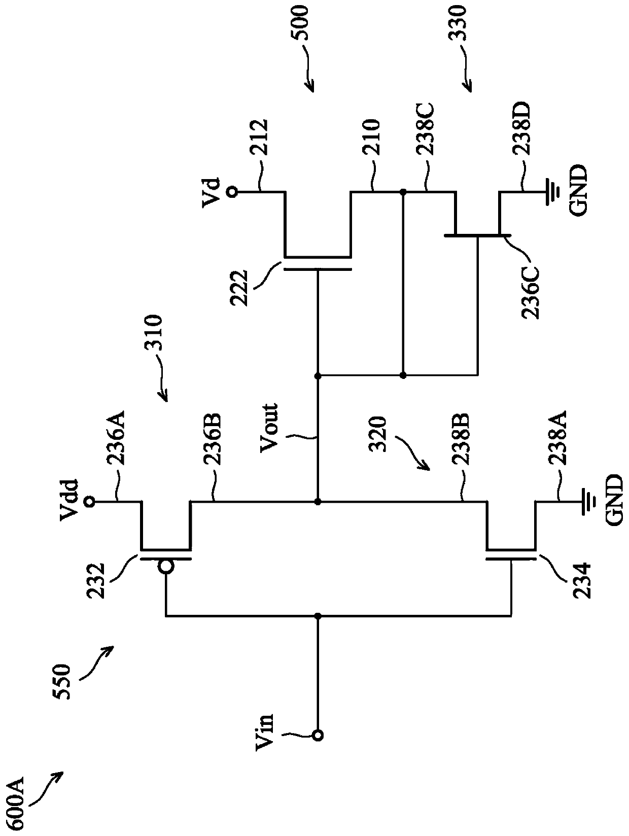
[0048] An embodiment of the present invention provides a semiconductor device, such as an enhancement mode (E-mode) high electron mobility transistor (HEMT)). The semiconductor device according to the embodiment of the present invention uses the gate stack of the flash memory as the gate struct...


PUM


Abstract

The embodiment of the invention provides a semiconductor device and a semiconductor structure. The semiconductor device includes a substrate, a first III-V compound layer, a second III-V compound layer, a source, a drain and a gate stack structure. The first III-V compound layer is disposed on the substrate. The second III-V compound layer is disposed on the first III-V compound layer. The sourceand the drain are disposed on opposite sidewall boundaries of the second III-V compound layer. The gate stack structure is disposed on the second III-V compound layer. The gate stack structure includes a first gate and a second gate. The first gate is disposed on the second III-V compound layer. The second gate is disposed on and electrically isolated from the first gate. The second gate is electrically coupled to the source.

Description

technical field [0001] Embodiments of the present invention relate to a semiconductor device and a semiconductor structure, in particular to an enhanced high electron mobility transistor device and a semiconductor structure including the enhanced high electron mobility transistor device. Background technique [0002] A high electron mobility transistor (HEMT) is a field effect transistor that uses a junction formed of two materials with different band gaps as a carrier channel. Compared with existing transistors, Gallium Nitride (GaN) HEMTs have excellent high-frequency performance, so they can operate in high-frequency ranges such as millimeter wave frequencies (millimeter wave frequencies), so they can be applied to mobile phones (cell phones) ), satellite television receivers, voltage converters or radar equipment and other high-frequency electronic products. However, the performance of current high electron mobility transistors needs to be further improved. [0003] Th...

Claims


Application Information

Patent Timeline
IPC IPC(8): H01L29/778H01L29/423
CPCH01L29/7786H01L29/7787H01L29/4232H01L29/788H01L29/808H01L29/861H01L21/823857H01L21/8252H01L27/0922H01L27/098H01L29/2003H01L29/66462H01L29/1066H01L29/7781H01L29/432
Inventor 韦维克陈柏安
Owner NUVOTON
Learn More