nand type rom

A technology of MOS transistors and memory cells, applied in the field of NAND read-only memory, can solve the problems of bit line BL voltage drop, bit line voltage drop, bit line read voltage drop, etc., to eliminate the drop of bit line voltage, Effect of eliminating bit line voltage drop and facilitating low-voltage operation

Active Publication Date: 2020-10-09
SHANGHAI HUALI INTEGRATED CIRCUTE MFG CO LTD
View PDF20 Cites 0 Cited by
  • Summary
  • Abstract
  • Description
  • Claims
  • Application Information

AI Technical Summary

Problems solved by technology

With the reduction of the operating voltage, that is, the power supply voltage, the reading voltage of the bit line caused by the leakage of the bit line drops very severely, especially in the FF process corner and high temperature conditions such as 125°C. The reading voltage of the bit line caused by the leakage of the bit line is very serious.
[0029] like Figure 2B As shown, it is a schematic diagram of the reduction of the bit line voltage caused by the bit line charge sharing of the existing NAND type ROM. Figure 2B Take the reading of the storage unit 102 in the storage unit series structure corresponding to the dotted line box 103c as an example for illustration. It can be seen that each of the storage units 102 in the storage unit series structure 103c between the drain and the low has a parasitic capacitance C CS , during the read process, the capacitance C corresponding to the bit line BL[0] BS The stored charge will be shared to the capacitor C CS In this way, the voltage of the bit line BL[0] will drop

Method used


Image

  • nand type rom
  • nand type rom
  • nand type rom

Examples


Embodiment Construction

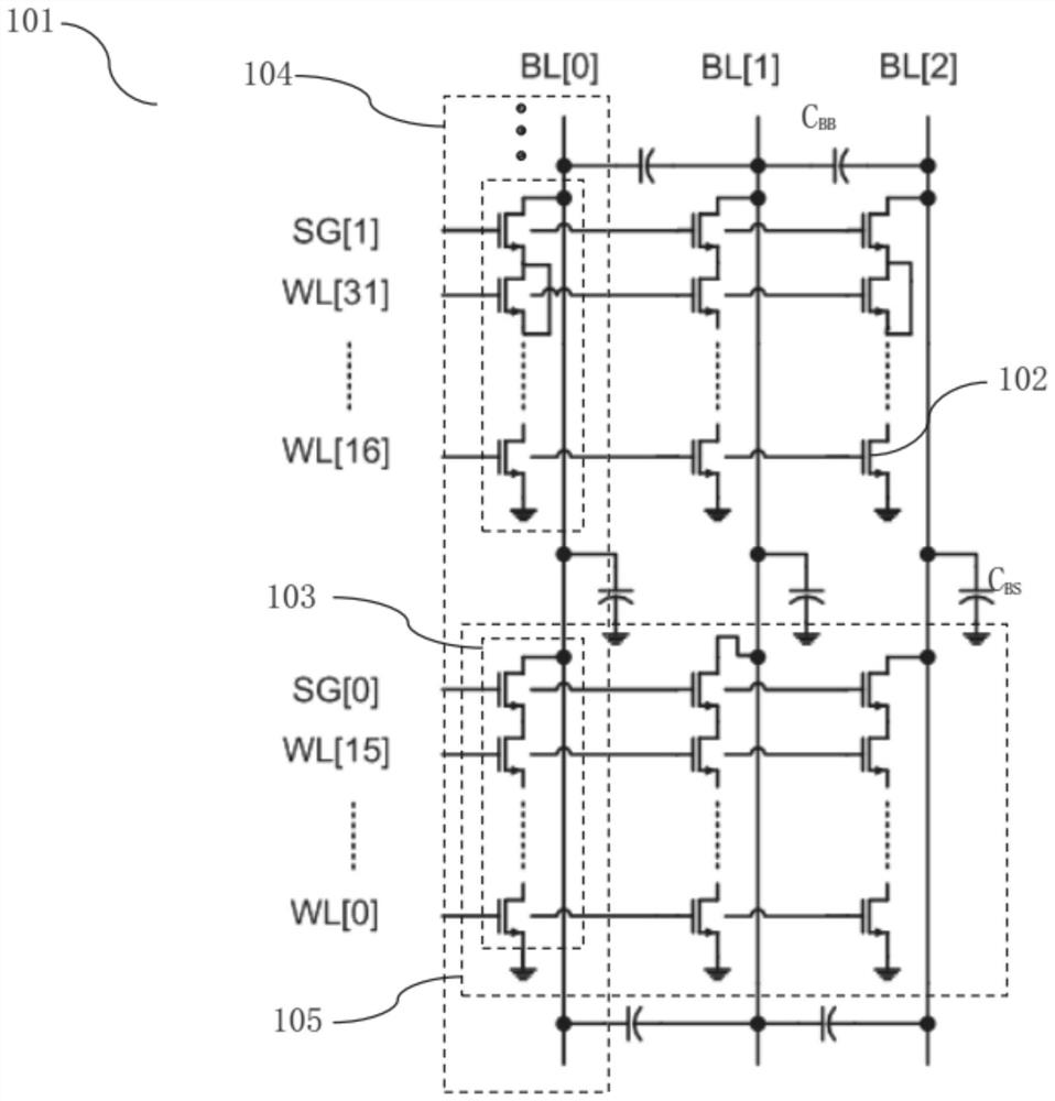
[0077] Such as Figure 3A Shown is the array structure 1 figure of NAND type ROM of the embodiment of the present invention, Figure 3B yes Figure 3A In the serial structure diagram of storage cells, the NAND-type ROM of the embodiment of the present invention includes an array structure 1 formed by a plurality of storage cells 2 arranged in rows and columns, and the column structure 4 of the array structure 1 includes:

[0078] A series structure 3 of multiple NAND type memory cells and a bit line. Figure 3A In the above, the bit line is represented by BL, and the bit line of different columns is represented by the number of columns, such as BL[0], BL[1], BL[2], BL[3], BL[4], BL[5] Show.

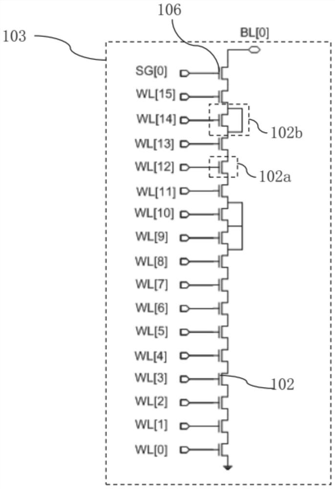
[0079] Such as Figure 3B As shown, each storage unit series structure 3 is formed by a selection transistor 6 and a plurality of storage units 2 in series.

[0080] The top node of each memory cell series structure 3 is connected to the bit line, such as Figure 3B BL[0] in .

[0...


PUM


Abstract

The invention discloses an NAND type ROM. A column structure comprises a plurality of NAND type memory cell series structures and bit lines. Each storage unit series structure is connected between thecorresponding bit line and the corresponding source line; each memory cell series structure in the row structure forms a corresponding memory cell series structure row; the source lines form a dynamic split type source electrode bias voltage structure, and specifically, any two adjacent storage unit series structures in the storage unit series structure row are connected with different source lines; source lines connected with different memory cell series structures in the same column are different. The bias voltage in the reading process is set as follows: the source line corresponding to the read memory cell is connected with a low level, the source line corresponding to the memory cell series structure adjacent to the read memory cell in the same row is connected with a high level, andthe source line corresponding to the memory cell series structure adjacent to the read memory cell in the same column structure is connected with a high level. The reading voltage drop caused by bitline electric leakage, bit line capacitance sharing and bit line crosstalk can be eliminated.

Description

technical field [0001] The invention relates to a semiconductor integrated circuit, in particular to a NAND type read-only memory (ROM). Background technique [0002] Such as Figure 1A Shown is the array structure 101 diagram of the existing NAND type ROM, Figure 1B yes Figure 1A In the serial structure diagram of memory cells in , the existing NAND-type ROM includes an array structure 101 formed by a plurality of memory cells 102 arranged in rows and columns, and the column structure 104 of the array structure 101 includes: [0003] A plurality of NAND-type memory cells are connected in series (string) structure 103 and a bit line. Figure 1A In the above, the bit line is represented by BL, and the bit line of different columns is represented by the number of columns, such as BL[0], BL[1], BL[2], BL[3], BL[4], BL[5] Show. [0004] Such as Figure 1B As shown, each storage unit series structure 103 is formed by a selection transistor 106 and a plurality of storage unit...

Claims


Application Information

Patent Timeline
Patent Type & Authority Patents(China)
IPC IPC(8): G11C5/06G11C16/26G11C16/08
CPCG11C5/063G11C16/08G11C16/26
Inventor 张适纬
Owner SHANGHAI HUALI INTEGRATED CIRCUTE MFG CO LTD
Why Eureka
Try Eureka