Superconducting digital circuit design method

A technology of digital circuits and design methods, applied in the fields of electrical digital data processing, computing, special data processing applications, etc., can solve the problems of low accuracy of timing analysis of superconducting digital circuits, avoid resource consumption, reduce area, and improve integration. degree of effect

Active Publication Date: 2019-07-19
SHANGHAI INST OF MICROSYSTEM & INFORMATION TECH CHINESE ACAD OF SCI
View PDF3 Cites 3 Cited by
  • Summary
  • Abstract
  • Description
  • Claims
  • Application Information

AI Technical Summary

Problems solved by technology

[0004] In view of the above-mentioned shortcoming of the prior art, the purpose of the present invention is to provide a superconducting digital circuit design method, which is used to solve the problems caused by the same supe

Method used


Image

  • Superconducting digital circuit design method
  • Superconducting digital circuit design method
  • Superconducting digital circuit design method

Examples


Embodiment 1

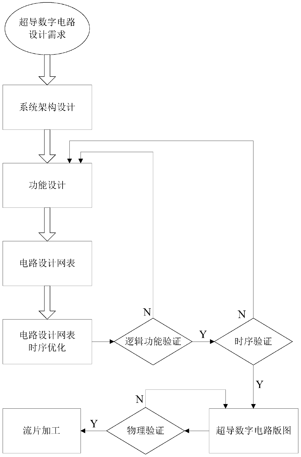
[0038] Such as figure 1 As shown, this embodiment provides a superconducting digital circuit design method, the design method includes:

[0039] Step 1: Based on the design requirements of the superconducting digital circuit, the system architecture design and function design are performed to generate a circuit design netlist.

[0040] As an example, the system architecture design is a structural design performed by superconducting digital circuit designers according to design requirements, that is, superconducting digital circuits are described as several typical logic devices connected to each other, wherein typical logic devices include arithmetic operation units ( adders, multipliers, etc.), registers, counters, etc. It should be noted that the system architecture designs completed by superconducting digital circuit designers according to different design requirements are different, and the system architecture designs completed by different superconducting digital circuit...

Embodiment 2

[0061]The difference between this embodiment and the first embodiment is that in the first embodiment, the magnetic flux storage capacity of the ports of each unit circuit is first judged when the unit library is established, so as to judge the ports with the magnetic flux storage capacity through the magnetic flux flag. Then, in step 2, identify whether the port of each unit circuit in the data path has the magnetic flux storage capacity through the magnetic flux flag. However, in this embodiment, the existing unit library is directly used, and then in step 2, the magnetic flux storage capacity of the ports of each unit circuit in the data path is directly judged to realize the detection. The specific methods include: based on the working principle of each unit circuit Judging whether the nearest Josephson junction connected in parallel with each port is located in the magnetic flux storage loop, and detecting that the port has a magnetic flux storage capability when the neare...


PUM


Abstract

The invention provides a superconducting digital circuit design method. The method comprises the steps of performing system architecture design and function design based on design requirements of a superconducting digital circuit, and then generating a circuit design netlist; performing magnetic flux storage capacity detection on all ports of all unit circuits on any data path in the circuit design netlist, and when the ports have the magnetic flux storage capacity, adding a buffer unit at the port to optimize the time sequence of the circuit design netlist, thereby obtaining a terminal circuit design netlist; and performing logic function verification and time sequence verification on the terminal circuit design netlist to generate a superconductive digital circuit layout, and performingphysical verification on the superconductive digital circuit layout to complete the design of the superconductive digital circuit. According to the invention, the problem that the time sequence analysis accuracy of the superconducting digital circuit is lower due to the fact that different loads are connected behind the same superconducting digital unit circuit when the superconducting digital circuit is designed by adopting a unit library design method in the prior art is solved.

Description

technical field [0001] The invention relates to the field of superconducting digital circuits, in particular to a design method for superconducting digital circuits. Background technique [0002] Single Flux Quantum (SFQ: Single Flux Quantum) is a superconducting circuit technology that uses a single flux quantum in a Josephson junction to represent logic "1" and "0". The clock frequency of superconducting digital circuits based on this can reach 770GHz, can be used for ultra-wideband analog-to-digital / digital-to-analog converters for radar and communication systems, broadband network switches, digital autocorrelators for radio astronomy, and superconducting computers. [0003] When extracting the timing characteristic parameters of a superconducting digital unit circuit, it is found that when the same superconducting digital unit circuit is connected to different loads, it will show different timing characteristic parameters (such as the delay of the superconducting digital...

Claims


Application Information

Patent Timeline
IPC IPC(8): G06F17/50
CPCG06F30/398
Inventor 王镇李秀婷高小平任洁应利良
Owner SHANGHAI INST OF MICROSYSTEM & INFORMATION TECH CHINESE ACAD OF SCI
Why Eureka
Try Eureka