Mask device, method for preparing OLED device and method for preparing OLED display panel
A mask plate and equipment technology, which is applied in semiconductor/solid-state device manufacturing, electric solid-state devices, semiconductor devices, etc., can solve the problems of poor display of OLED display panels, prolonged evaporation process consumption, and easy generation of particles, etc., to achieve improved The effect of displaying quality, shortening consumption time, and avoiding pollution
- Summary
- Abstract
- Description
- Claims
- Application Information
AI Technical Summary
Problems solved by technology
Method used
Image

Examples
no. 1 example
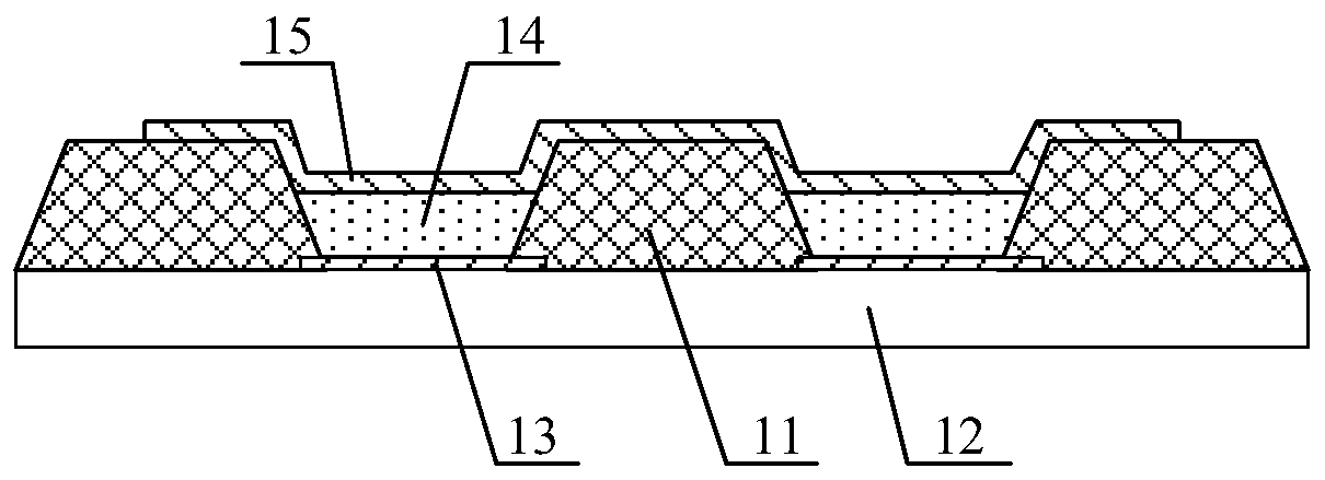
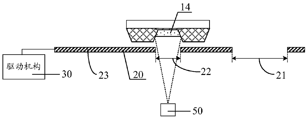
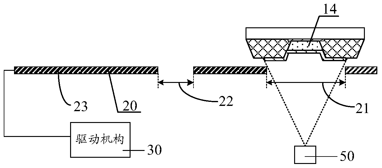
[0039] figure 2 It is a schematic structural diagram of a masking device according to an embodiment of the present invention. Such as figure 2 As shown, the masking apparatus of the embodiment of the present invention includes a mask plate 20 and a driving mechanism 30 for driving the mask plate 20 to move. A plurality of mask patterns are disposed on the mask plate 20 . The driving mechanism 30 drives the mask plate 20 to move so that one of the mask patterns corresponds to a position to be evaporated, so as to perform different evaporation states.
[0040] In the masking equipment of the embodiment of the present invention, the mask plate 20 is provided with a plurality of mask patterns, and the mask plate 20 is driven to move by the driving mechanism 30, so that one of the mask patterns corresponds to the position to be evaporated, so as to perform different evaporation state. Therefore, when switching between different evaporation states, only the driving mechanism i...
no. 2 example
[0052] Based on the inventive concepts of the foregoing embodiments, the second embodiment of the present invention provides a method for preparing an OLED device, which uses the mask equipment in the above embodiment to evaporate and form an OLED device, and the method includes:
[0053] The driving mechanism drives the movement of the mask plate, so that the second hollow structure corresponds to the position of the OLED device, and the organic light-emitting layer is formed by evaporation;
[0054] The driving mechanism drives the movement of the mask plate, so that the first hollow structure corresponds to the position of the OLED device, and the cathode layer is formed by evaporation.
[0055] The method also includes:
[0056] When another OLED device is formed by evaporation, the driving mechanism drives the mask to move so that the physical shielding part corresponds to the position of the current OLED device, so as to shield the current OLED device.
no. 3 example
[0058] Based on the inventive concepts of the foregoing embodiments, the third embodiment of the present invention provides a method for preparing an OLED display panel, including:
[0059] providing a substrate;
[0060] The OLED device was prepared on the substrate by using the method of the above-mentioned embodiment.
[0061] The display panel can be any product or component with a display function such as a mobile phone, a tablet computer, a TV set, a monitor, a notebook computer, a digital photo frame, a navigator, and the like.
PUM
 Abstract
Description
Claims
Application Information
 - R&D Engineer
- R&D Manager
- IP Professional
- Industry Leading Data Capabilities
- Powerful AI technology
- Patent DNA Extraction
Browse by: Latest US Patents, China's latest patents, Technical Efficacy Thesaurus, Application Domain, Technology Topic.
© 2024 PatSnap. All rights reserved.Legal|Privacy policy|Modern Slavery Act Transparency Statement|Sitemap