High-resistance buffer layer using gan-based narrow well multiple quantum well structure and preparation method

A multi-quantum well structure and high-resistance buffer layer technology, which is applied in semiconductor/solid-state device manufacturing, semiconductor devices, electrical components, etc., can solve the problems of epitaxial layer quality deterioration, mobility decline, poor repeatability, etc., and achieve high resistance value, the effect of reducing leakage

Active Publication Date: 2022-07-29
QUANZHOU SANAN SEMICON TECH CO LTD
View PDF0 Cites 0 Cited by
  • Summary
  • Abstract
  • Description
  • Claims
  • Application Information

AI Technical Summary

Problems solved by technology

The first method is to obtain a high-resistance GaN epitaxial layer by introducing defect impurities, so the quality of the epitaxial layer will deteriorate. At the same time, the method of obtaining high-resistance GaN by controlling growth conditions is highly dependent on equipment and poor in repeatability; The introduction of metal impurities in the second method has a strong memory effect and will always remain in the reaction chamber, making subsequent epitaxial materials have the risk of being contaminated by metal impurities. Therefore, it is generally necessary to have a dedicated MOCVD to grow high resistance GaN-based epitaxial materials and introduce Impurities will reduce the mobility of channel 2DEG and affect device characteristics

Method used


Image

  • High-resistance buffer layer using gan-based narrow well multiple quantum well structure and preparation method
  • High-resistance buffer layer using gan-based narrow well multiple quantum well structure and preparation method
  • High-resistance buffer layer using gan-based narrow well multiple quantum well structure and preparation method

Examples


Embodiment Construction

[0025] The present invention will be described in detail below with reference to the specific drawings and embodiments.

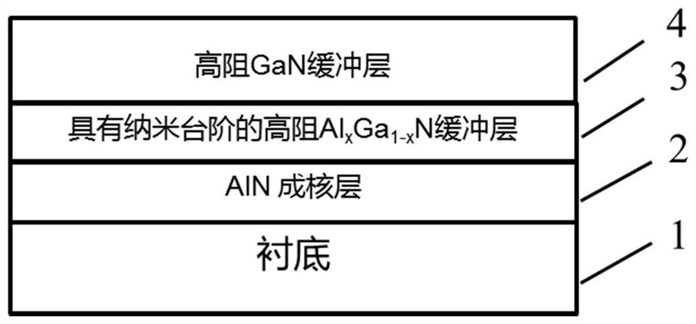
[0026] refer to Figure 1-2 , a high-resistance buffer layer utilizing a GaN-based narrow well multiple quantum well structure, comprising a Si or SiC substrate 1, an AlN nucleation layer 2, Al a Ga 1-aN-based narrow well multiple quantum well high resistance buffer layer 3 and high resistance GaN buffer layer 4:

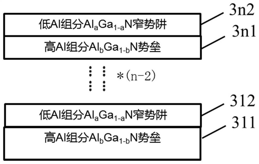
[0027] the Al a Ga 1-a The N-based narrow well multiple quantum well high resistance buffer layer 3 includes a plurality of quantum well periods, and each quantum well period further includes stacked low Al composition Al a Ga 1-a N narrow well layer 311...3n1, high Al composition Al b Ga 1-b N barrier layers 312...3n2, the number of multi-quantum periods is 5-100; the high Al composition Al b Ga 1-b The thickness of the N barrier layer is larger than that of the low Al composition Al a Ga 1-a N thickness of the narrow well layer.

[...


PUM

PropertyMeasurementUnit
thicknessaaaaaaaaaa
thicknessaaaaaaaaaa
thicknessaaaaaaaaaa

Abstract

The invention provides a high-resistance buffer layer using a GaN-based narrow well multiple quantum well structure and a preparation method, including a substrate, a nucleation layer, an Al a Ga 1‑a N-based narrow well multiple quantum well high resistance buffer layer and GaN buffer layer: Al a Ga 1‑a The N-based narrow well multi-quantum well high-resistance buffer layer includes a plurality of multi-quantum well structure stress transfer layers, and the Al content in the multi-quantum well structure stress transfer layers decreases sequentially from bottom to top; each multi-quantum well structure stress transfer layer It further includes a plurality of quantum well periods, and each quantum well period further includes stacked low Al composition Al a Ga 1‑ a N narrow well layer, high Al composition Al b Ga 1‑b N barrier layer, the number of multi-quantum periods is 5‑100; high Al composition Al b Ga 1‑b The thickness of the N barrier layer is larger than that of the low Al composition Al a Ga 1‑a N thickness of the narrow well layer.

Description

technical field [0001] The present invention relates to an electronic component, in particular to a field effect transistor. Background technique [0002] The growth of high-quality semi-insulating GaN-based buffer layers has always been the key technology for epitaxial growth of GaN-based High Electron Mobility Transistor (HEMT) devices. When the HEMT device is working, the leakage of the GaN-based buffer layer will not only deteriorate the pinch-off performance of the device, but also weaken the gate's ability to control the channel current, thereby deteriorating the overall performance of the device; at the same time, the leakage in the buffer layer will also increase the device. Therefore, the leakage of the GaN-based buffer layer has always been a difficult problem to improve the performance of HEMT devices. In order to obtain good device characteristics and improve device reliability, a high-resistance GaN-based buffer layer must be grown to reduce parasitic leakage c...

Claims


Application Information

Patent Timeline
Patent Type & Authority Patents(China)
IPC IPC(8): H01L29/778H01L21/335H01L29/15H01L29/20
CPCH01L29/66462H01L29/778H01L29/15H01L29/151H01L29/2003
Inventor 房育涛刘波亭张恺玄
Owner QUANZHOU SANAN SEMICON TECH CO LTD
Why Eureka
Try Eureka