Post-binding through silicon via test structure and method specific to through silicon via electric leakage fault

A test structure and through-silicon via technology, which is applied in the direction of measuring electricity, measuring devices, measuring electrical variables, etc., can solve the problems of small measurement error, low measurement accuracy, and failure to determine the fault point, and achieve test cost reduction and small leakage area. Effect

Inactive Publication Date: 2019-07-26
HARBIN INST OF TECH
View PDF11 Cites 0 Cited by
  • Summary
  • Abstract
  • Description
  • Claims
  • Application Information

AI Technical Summary

Problems solved by technology

[0008] The present invention aims to solve the problems of low measurement accuracy of the traditional TSV test structure, small measurement error when there is an error fault, and failure to determine the fault point, and now provides a bonded TSV test for TSV leakage faults structure and method

Method used


Image

  • Post-binding through silicon via test structure and method specific to through silicon via electric leakage fault
  • Post-binding through silicon via test structure and method specific to through silicon via electric leakage fault
  • Post-binding through silicon via test structure and method specific to through silicon via electric leakage fault

Examples


specific Embodiment approach 1

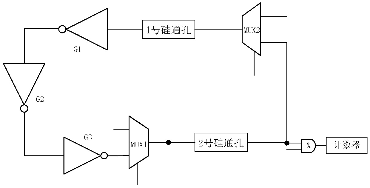
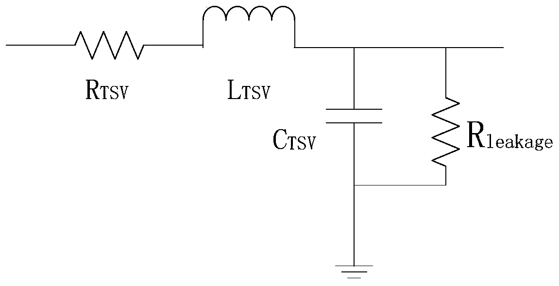
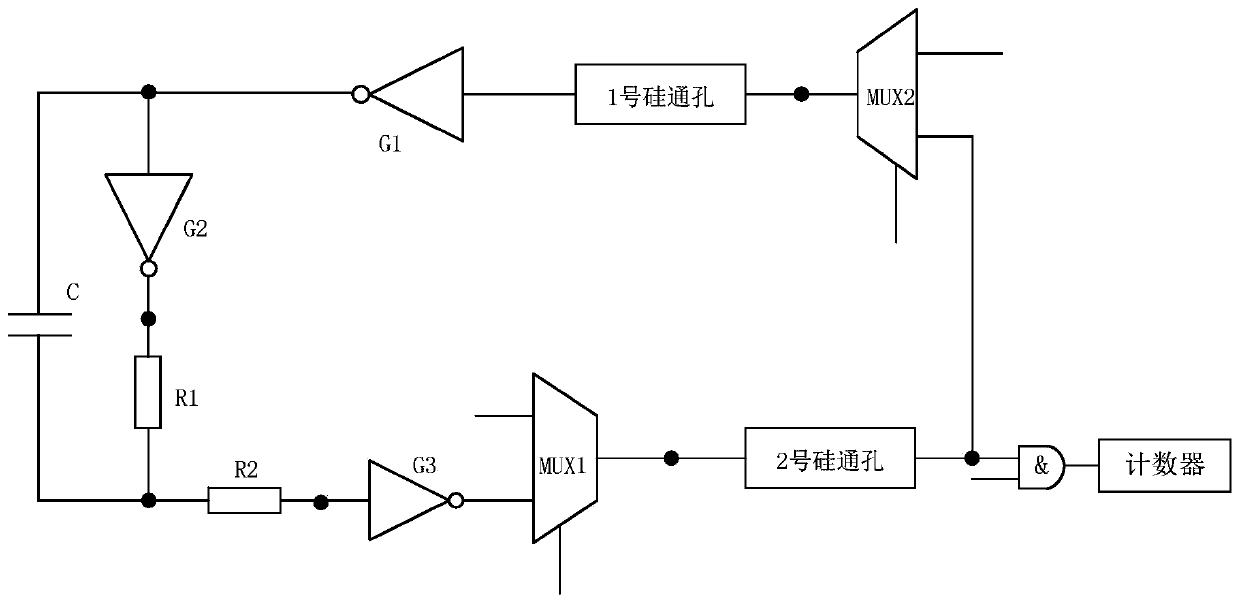
[0032] Specific implementation mode one: refer to Figures 1 to 4 This embodiment is described in detail. A bonded TSV test structure for TSV leakage faults described in this embodiment includes a traditional TSV test circuit based on a ring oscillator and a circuit for reducing the ring oscillator frequency of the RC circuit.

[0033] The above-mentioned traditional ring oscillator-based TSV test circuit includes: selector MUX1, selector MUX2, inverter G1, inverter G2, inverter G3, AND gate circuit and counter; RC circuit includes: capacitor C , resistor R1 and resistor R2.

[0034] The signal output terminal of the selector MUX2 is connected to one end of the No. 1 TSV, the other end of the No. 1 TSV is connected to the signal input end of the inverter G1, and the signal output end of the inverter G1 is simultaneously connected to the signal of the inverter G2 The input end and one end of the capacitor C, the signal output end of the inverter G2 is connected to one end of ...

specific Embodiment approach 2

[0041] Specific implementation mode 2: A binding TSV test method for TSV leakage faults described in this embodiment mode, the method is realized by a TSV test circuit based on a ring oscillator, and the TSV test circuit Including: selector MUX1, selector MUX2, inverter G1, inverter G2, inverter G3, AND gate circuit, counter, capacitor C, resistor R1 and resistor R2.

[0042] The signal output terminal of the selector MUX2 is connected to one end of the No. 1 TSV, the other end of the No. 1 TSV is connected to the signal input end of the inverter G1, and the signal output end of the inverter G1 is simultaneously connected to the signal of the inverter G2 The input end and one end of the capacitor C, the signal output end of the inverter G2 is connected to one end of the resistor R1, the other end of the resistor R1 and the other end of the capacitor C are connected to one end of the resistor R2 at the same time, and the other end of the resistor R2 is connected to the inverter ...


PUM


Abstract

The invention discloses a post-binding through silicon via test structure and method specific to a through silicon via electric leakage fault, relates to the field of integrated circuit test, and aimsto solve the problems of low measurement accuracy, low measurement error in case of an error fault and incapability of determining a fault point in a conventional through silicon via test structure.The post-binding through silicon via test structure and method specific to the through silicon via electric leakage fault comprises a conventional through silicon via test circuit based on a ring oscillator, and a RC circuit used for lowering the frequency of the ring oscillator. Specific to the post-binding test of a through silicon via, the detected fault is determined as the electric leakage fault of the through silicon via. When the through silicon via is connected, the signal outputting period of the test structure is more sensitive to the electric leakage fault of the through silicon via, so that the test cost is lowered, and the influence of the diagnosis result on the measurement error is smaller. The post-binding through silicon via test structure is suitable for detecting micro electric leakage area.

Description

technical field [0001] The invention belongs to the field of integrated circuit testing. Background technique [0002] Moore's Law predicts that when the price remains constant, the number of components that can be accommodated on an integrated circuit will double approximately every 18-24 months. This trend has been going on for half a century, but as the physical size of complementary metal-oxide-semiconductor (CMOS) transistors is gradually approaching the limit, it is no longer reasonable to rely solely on reducing the size of transistors to improve the performance of integrated circuits. Therefore, relying on shrinking transistor size to improve integrated circuit performance and reduce power consumption has become unfeasible. The traditional two-dimensional integrated circuit process can no longer meet the requirements of today's industry for high processing speed and low power consumption of integrated circuits. Three-dimensional integrated circuits are considered t...

Claims


Application Information

Patent Timeline
Patent Type & Authority Applications(China)
IPC IPC(8): G01R31/02
CPCG01R31/50
Inventor 俞洋杨智明徐康康彭喜元
Owner HARBIN INST OF TECH
Why Eureka
Try Eureka