Flexible OLED device thin film packaging method

A thin-film packaging and device technology, which is applied in the manufacture of electrical solid devices, semiconductor devices, semiconductor/solid devices, etc., can solve the problems of poor water and oxygen barrier performance, easy cracks and falling off, serious stress mismatch, etc., to achieve Improve water and oxygen barrier performance, reduce stress, and have good packaging effect

Active Publication Date: 2019-07-26
FUZHOU UNIV
View PDF13 Cites 3 Cited by
  • Summary
  • Abstract
  • Description
  • Claims
  • Application Information

AI Technical Summary

Problems solved by technology

However, due to the porous structure of most organic matter, its water and oxygen barrier performance itself is not very good
On the other hand, the stress mismatch between the organic layer and the inorganic layer is relatively serious, which makes it easy to generate cracks and fall off during the bending process, and damage the device

Method used


Image

  • Flexible OLED device thin film packaging method
  • Flexible OLED device thin film packaging method
  • Flexible OLED device thin film packaging method

Examples


Embodiment 1

[0034] A thin-film packaging method for a flexible OLED device, using an inorganic / organic overlapping packaging layer, modifying the surface of the organic barrier layer of the packaging layer, and setting a sacrificial layer in the packaging structure, and the packaging structure is periodically repeated;

[0035] The packaging method comprises the steps of:

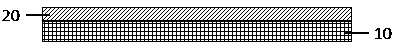
[0036] (1) As attached figure 1 As shown, a pre-prepared OLED device 10 is provided, and an inorganic barrier layer 20 is prepared on the surface of the pre-prepared OLED device 10 by atomic layer deposition;

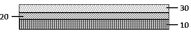
[0037] (2) As attached figure 2 As shown, an organic barrier layer 30 is prepared on the surface of the inorganic barrier layer 20 in step (1);

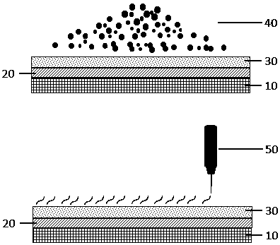
[0038] (3) As attached image 3 As shown, the surface of the organic barrier layer 20 is treated with plasma 40;

[0039] (4) As attached Figure 4 As shown, repeat steps (1) to (3) once, and then sequentially prepare the inorganic barrier layer 21 and the organi...


PUM


Abstract

The invention relates to a flexible OLED (Organic Light Emitting Diode) device thin film packaging method. According to the thin film packaging method, an inorganic/organic overlapping packaging structure is adopted, and the surface of each organic layer of the packaging structure is modified, so that the surfaces become hydrophobic, the size and quantity of pinholes are reduced, the water-oxygenisolation performance of the packaging structure is improved, and meanwhile stress between each inorganic layer and each organic layer is reduced; and the steps are repeated periodically, and a sacrificial layer is arranged in the packaging structure, so that the water-oxygen isolation performance of the packaging structure is further improved. Through the method, process procedures are simple, and the packaging effect is good.

Description

technical field [0001] The invention belongs to the field of thin film packaging of organic photoelectric devices, and in particular relates to a thin film packaging method for flexible OLED devices. Background technique [0002] In recent years, organic light emitting diode (Organic Light Emitting Diode) display technology has developed rapidly and has been widely used. Due to its own series of advantages, OLED is recognized as the next generation mainstream display technology. However, the organic materials used in OLED displays and the cathode metal materials are prone to reactions to water vapor and oxygen, and the device stability and service life are restricted. Therefore, the better the packaging effect of the device, the longer the service life of the device will be. [0003] There are two encapsulation methods currently in use. One is to use glass packaging or metal cover packaging. In an inert gas environment, the cover and the OLED device are bonded with encaps...

Claims


Application Information

Patent Timeline
Patent Type & Authority Applications(China)
IPC IPC(8): H01L51/52H01L51/56
CPCH10K71/135H10K71/164H10K71/12H10K50/84H10K71/00
Inventor 周雄图孙钒张永爱郭太良唐谦林志贤杨尊先叶芸
Owner FUZHOU UNIV
Why Eureka
Try Eureka