Thin film packaging structure and preparation method and application thereof

A technology of thin-film packaging and packaging structure, which is applied in semiconductor/solid-state device manufacturing, electrical components, electric solid-state devices, etc., to achieve good stress release space, improved heat insulation performance, and better flexibility

Pending Publication Date: 2022-03-01
GUANGDONG JUHUA PRINTING DISPLAY TECH CO LTD
View PDF0 Cites 0 Cited by
  • Summary
  • Abstract
  • Description
  • Claims
  • Application Information

AI Technical Summary

Problems solved by technology

[0005] Based on this, it is necessary to provide a composite thin film flexible packaging structure that can solve the interface defects of the multilayer thin film structure and better prevent water and oxygen penetration, and its preparation method and use

Method used


Image

  • Thin film packaging structure and preparation method and application thereof
  • Thin film packaging structure and preparation method and application thereof
  • Thin film packaging structure and preparation method and application thereof

Examples


preparation example Construction

[0037] The present invention also provides a method for preparing the thin film encapsulation structure, comprising the following steps:

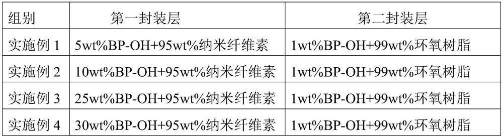
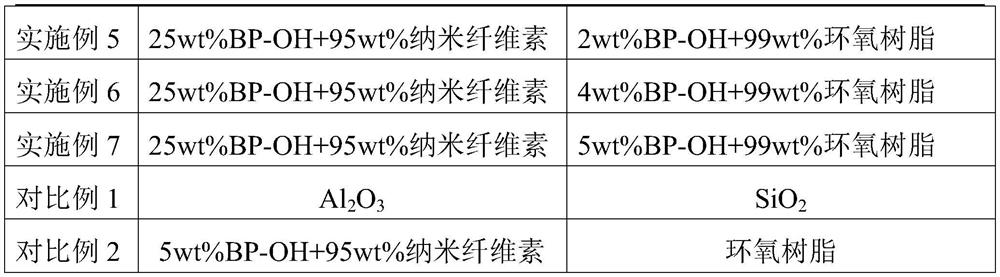
[0038] S10, providing the modified layered two-dimensional material, and mixing the modified layered two-dimensional material and the nanocellulose to obtain a first mixture, dissolving the first mixture in a solvent to form a the ink of the first mixture, and inkjet printing the ink containing the first mixture on the structure to be encapsulated to form a first encapsulation layer;

[0039] S20, mixing the modified layered two-dimensional material and the polymer water-repelling oxygen film-forming material to obtain a second mixture, dissolving the first mixture in a solvent to form an ink containing the second mixture, Inkjet printing an ink containing the second mixture on the first encapsulation layer to form a second encapsulation layer.

[0040] The modified layered two-dimensional material can be prepared by exfoliating the layere...

Embodiment 1

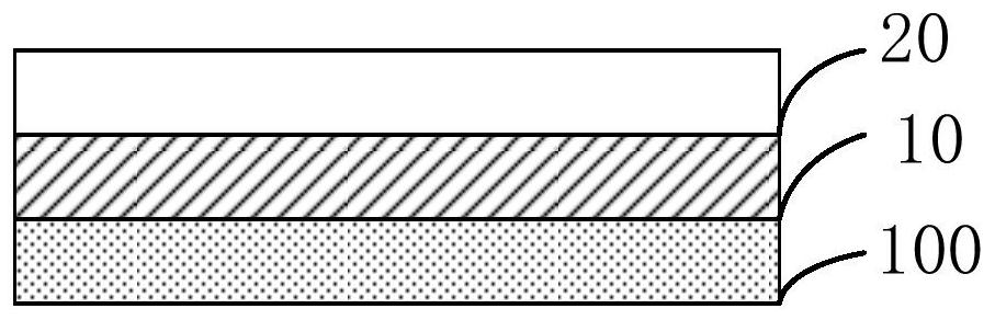
[0055] A QLED device, including an anode and a cathode, an organic functional layer between the anode and the cathode, and a thin-film packaging structure covering the cathode, specifically: ITO substrate / PEDOT:PSS(50nm) / poly-TPD(30nm) / Quantum dot light-emitting layer (20nm) / ZnO(30nm) / silver (70nm) / thin film encapsulation structure (540nm), wherein the thin film encapsulation structure is composed of the first encapsulation layer and the second encapsulation layer, the first encapsulation layer is BP-OH / The NFC composite film has a thickness of 260nm, and the second packaging layer is a BP-OH / epoxy resin composite film with a thickness of 280nm. BP-OH is modified black phosphorus with hydroxyl groups on the surface, and NFC is nanocellulose. The specific preparation method of the thin film encapsulation structure is as follows:

[0056] (1) Preparation of BP-OH: The two-dimensional material BP was peeled off by ball milling with the assistance of LiOH. The ball milling spee...

Embodiment 2

[0060] A QLED device, including an anode and a cathode, an organic functional layer between the anode and the cathode, and a thin-film packaging structure covering the cathode, specifically: ITO substrate / PEDOT:PSS(50nm) / poly-TPD(30nm) / Quantum dot light-emitting layer (20nm) / ZnO(30nm) / silver (70nm) / thin film encapsulation structure (540nm), wherein the thin film encapsulation structure is composed of the first encapsulation layer and the second encapsulation layer, the first encapsulation layer is BP-OH / The NFC composite film has a thickness of 260nm, and the second packaging layer is a BP-OH / epoxy resin composite film with a thickness of 280nm. BP-OH is modified black phosphorus with hydroxyl groups on the surface, and NFC is nanocellulose. The specific preparation method of the thin film encapsulation structure is as follows:

[0061] (1) Preparation of BP-OH: The two-dimensional material BP was peeled off by ball milling with the assistance of LiOH. The ball milling spee...


PUM

PropertyMeasurementUnit
thicknessaaaaaaaaaa
thicknessaaaaaaaaaa
diameteraaaaaaaaaa

Abstract

The invention provides a thin film packaging structure. The thin film packaging structure comprises a first packaging layer used for covering a structure to be packaged; the second packaging layer is formed on the first packaging layer; wherein the first packaging layer comprises a modified layered two-dimensional material and nanocellulose, the second packaging layer comprises a modified layered two-dimensional material and a polymer water-blocking oxygen film-forming material, and the surface of the modified layered two-dimensional material contains hydroxyl or amino. And the content of the modified layered two-dimensional material in the first packaging layer is greater than or equal to that of the modified layered two-dimensional material in the second packaging layer. The invention also provides a preparation method of the thin film packaging structure. The invention further provides a light-emitting device which comprises the thin film packaging structure.

Description

technical field [0001] The invention relates to the field of packaging technology, in particular to a composite thin film flexible packaging structure and its preparation method and application. Background technique [0002] The lifetime of optoelectronic devices is a very important parameter. Encapsulation is a crucial link to improve the life of optoelectronic devices and make them reach commercial levels. For optoelectronic devices, encapsulation is not only physical protection to prevent scratches, but more importantly, to prevent the penetration of water vapor and oxygen in the external environment. Water vapor and oxygen in these environments penetrate into the device, which will accelerate the aging of the device. In addition, the device will generate a certain amount of heat during use, and a good packaging film also needs to have a certain heat resistance function. Therefore, the packaging structure of the optoelectronic device must have a good permeation barrier ...

Claims


Application Information

Patent Timeline
Patent Type & Authority Applications(China)
IPC IPC(8): H01L51/52H01L51/56
CPCH10K50/846H10K50/8426H10K50/844H10K71/00
Inventor 朱佩
Owner GUANGDONG JUHUA PRINTING DISPLAY TECH CO LTD
Why Eureka
Try Eureka