Display panel, manufacturing method thereof, and electronic device

A display panel and substrate technology, applied in the direction of circuits, electrical components, electrical solid devices, etc., to achieve the effects of large-scale industrial application, simple process, and low production cost

Active Publication Date: 2021-03-19
GUANGZHOU GOVISIONOX TECH CO LTD
View PDF3 Cites 0 Cited by
  • Summary
  • Abstract
  • Description
  • Claims
  • Application Information

AI Technical Summary

Problems solved by technology

However, there is still a lot of room for improvement in the packaging modules in the prior art

Method used


Image

  • Display panel, manufacturing method thereof, and electronic device
  • Display panel, manufacturing method thereof, and electronic device
  • Display panel, manufacturing method thereof, and electronic device

Examples


Embodiment Construction

[0039] The following will clearly and completely describe the technical solutions in the embodiments of the present invention with reference to the accompanying drawings in the embodiments of the present invention. Obviously, the described embodiments are only some of the embodiments of the present invention, not all of them. Based on the embodiments of the present invention, all other embodiments obtained by persons of ordinary skill in the art without making creative efforts belong to the protection scope of the present invention.

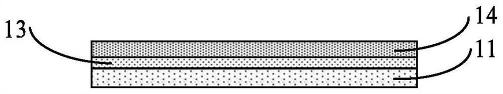
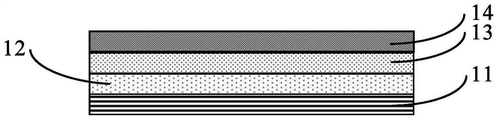
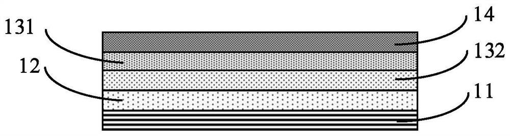
[0040] The polarizing layer of the display panel in the prior art is arranged outside the encapsulation structure. For example, for a flexible OLED display panel, its structure generally consists of a backplane film layer, an OLED device layer, a TFE layer, a TP (Touch) layer, a first adhesive layer, a polarizing layer, a second adhesive layer, and a cover layer.

[0041] Specifically, for a thin-film-encapsulated flexible OLED display panel, its...


PUM

PropertyMeasurementUnit
thicknessaaaaaaaaaa
thicknessaaaaaaaaaa
thicknessaaaaaaaaaa

Abstract

Embodiments of the present invention provide a display panel, a manufacturing method thereof, and an electronic device, which improve an existing packaging module of a display panel. Both the display panel and the electronic device include: a substrate, a light-emitting functional layer is disposed on the substrate, a first inorganic encapsulation layer disposed on the light-emitting functional layer, a polarizing layer disposed on the first inorganic encapsulation layer, The second inorganic encapsulation layer disposed on the polarizing layer improves the encapsulation performance of the flexible display panel by arranging the polarizing layer in the encapsulation structure; in addition, the preparation method of the display panel provided by the application adopts a process integration method, and the process The method is simple, low in production cost and high in production efficiency, and is conducive to large-scale industrial application.

Description

technical field [0001] The invention relates to the field of display technology, in particular to a display panel, a preparation method thereof, and electronic equipment. Background technique [0002] With the development of display technology and the improvement of human requirements for display screens, display products tend to be more flexible and thinner. Among them, OLED (Organic Light Emitting Diode, organic light emitting diode) has all solid state, ultra-thin, fast response, With the advantages of high luminous efficiency, high contrast, low power consumption, and easy realization of flexible display and 3D display, it is considered to be one of the most promising display technologies and has been widely used in electronic products such as mobile phone screens, computer monitors, and full-color TVs. . [0003] Since OLED light-emitting devices are easily corroded by water and oxygen, TFE (thin film encapsulation technology) is often used to isolate water and oxygen....

Claims


Application Information

Patent Timeline
Patent Type & Authority Patents(China)
IPC IPC(8): H01L27/32H01L51/52
CPCH10K59/00H10K50/84H10K50/868
Inventor 彭祥应如波
Owner GUANGZHOU GOVISIONOX TECH CO LTD
Why Eureka
Try Eureka