Display panel and making method thereof

A technology for display panels and manufacturing methods, applied in optics, instruments, electrical components, etc., can solve the problem that the frame size of display panels cannot be further reduced, and achieve the effects of narrow frames, reduced impedance, and space-saving utilization

Active Publication Date: 2019-08-06
HANNSTAR DISPLAY CORPORATION
View PDF14 Cites 11 Cited by
  • Summary
  • Abstract
  • Description
  • Claims
  • Application Information

AI Technical Summary

Problems solved by technology

[0003] The technical problem to be solved by the present invention is that the transfer structure of the wires in the prior art occupies a certain area, and the wires of different layers are respectively connected by non-overlapping contact holes and transfer pads that span two contact holes at the same time, thus causing The bezel size of the display panel cannot be further reduced

Method used


Image

  • Display panel and making method thereof
  • Display panel and making method thereof
  • Display panel and making method thereof

Examples


Embodiment Construction

[0115] In order to enable those skilled in the art to further understand the present invention, the preferred embodiments of the present invention are listed below, and the composition and desired effects of the present invention are described in detail with reference to the accompanying drawings. It should be noted that the drawings are all simplified schematic diagrams, therefore, only the components and combinations related to the present invention are shown to provide a clearer description of the basic structure or implementation method of the present invention, and the actual components and layout may be more accurate. for complex. In addition, for the convenience of description, the components shown in the drawings of the present invention are not drawn in proportion to the number, shape, and size of the actual implementation, and the detailed proportions can be adjusted according to design requirements.

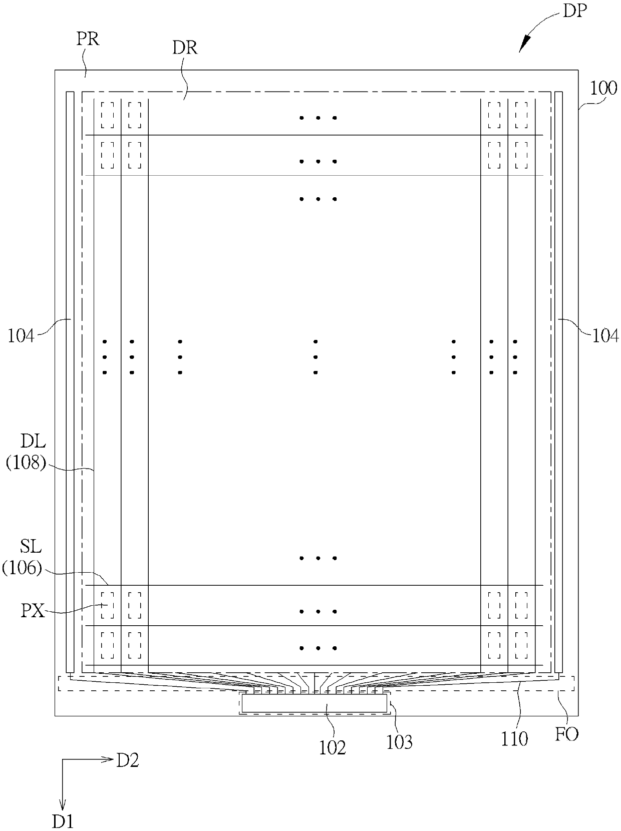
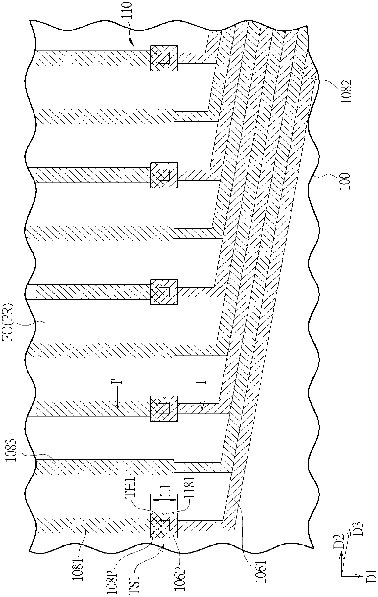
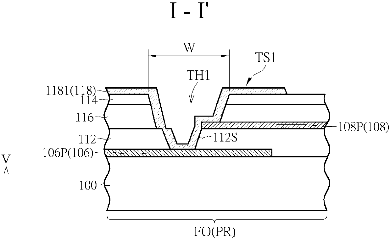
[0116] Please refer to Figure 1 to Figure 3 , figure 1 is a sc...


PUM


Abstract

The invention discloses a display panel comprising a first conductive layer, a first insulating layer, a second conductive layer, a second insulating layer, a first connecting hole and a first transparent conductive layer. The first conductive layer disposed on the substrate includes a first contact pad disposed in a peripheral region. The first insulating layer is disposed on the first conductivelayer. The second conductive layer is disposed on the first insulating layer and includes a second contact pad disposed in the peripheral region. The second insulating layer is disposed on the firstinsulating layer and the second conductive layer. The first connecting hole penetrates the first insulating layer and the second insulating layer and exposes one portion of the first contact pad and one portion of the second contact pad. The first transparent conductive layer is disposed on the second insulating layer and includes a first connection electrode covering the first connecting hole. Afirst connection electrode is in direct contact and is electrically connected with the first contact pad and the second contact pad through the first connecting hole; and the first connecting hole, the first contact pad, the second contact pad and the first connection electrode form a transfer structure.

Description

technical field [0001] The present invention relates to a display panel and a manufacturing method thereof, in particular to a display panel with a smaller occupied area of ​​a transition structure and a manufacturing method thereof. Background technique [0002] In the peripheral area of ​​the existing display panel, the wires can be composed of different conductive layers. In this case, the wires are respectively provided with contact pads in different conductive layers, and the contact pads of different conductive layers can be connected to each other through their corresponding connection holes, so that the wires can maintain electrical connection between different conductive layers. , so the transition between different conductive layers usually requires an area larger than two connection holes. In addition, the contact pads are also designed to have a certain area to ensure that the connection holes can be arranged corresponding to the contact pads. As the resolution...

Claims


Application Information

Patent Timeline
IPC IPC(8): G02F1/13G09F9/33H01L27/32
CPCG02F1/1303G09F9/33H10K59/00
Inventor 叶政谚
Owner HANNSTAR DISPLAY CORPORATION
Why Eureka
Try Eureka