
Infrared detector structure with high filling factor and manufacturing method thereof

An infrared detector and fill factor technology, applied in the field of infrared detectors, can solve the problems affecting the area ratio of the micro-bridge, affecting the performance of the detector, and decreasing the ratio of the micro-bridge area, so as to reduce the area, increase the fill factor, and improve the The effect of product performance

Active Publication Date: 2019-08-13
SHANGHAI INTEGRATED CIRCUIT RES & DEV CENT
View PDF14 Cites 7 Cited by
  • Summary
  • Abstract
  • Description
  • Claims
  • Application Information

AI Technical Summary

Problems solved by technology

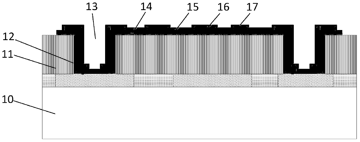
[0011] In the above-mentioned prior art, since the electrical connection hole 13 is located inside the support hole 12, that is, the structure of a large hole covering a small hole is adopted, so when the electrical connection hole 13 is photoetched, in order to ensure the implementation of the photoetching process , the size of the support hole 12 and the electrical connection hole 13 needs to be designed relatively large, which will affect the proportion of the micro-bridge area in the pixel area, resulting in a decrease in the proportion of the infrared-sensitive micro-bridge area, which affects the performance of the detector

Method used


Image

  • Infrared detector structure with high filling factor and manufacturing method thereof
  • Infrared detector structure with high filling factor and manufacturing method thereof

Examples


Embodiment Construction

[0037] The specific embodiment of the present invention will be further described in detail below in conjunction with the accompanying drawings.

[0038] It should be noted that, in the following specific embodiments, when describing the embodiments of the present invention in detail, in order to clearly show the structure of the present invention for the convenience of description, the structures in the drawings are not drawn according to the general scale, and are drawn Partial magnification, deformation and simplification are included, therefore, it should be avoided to be interpreted as a limitation of the present invention.

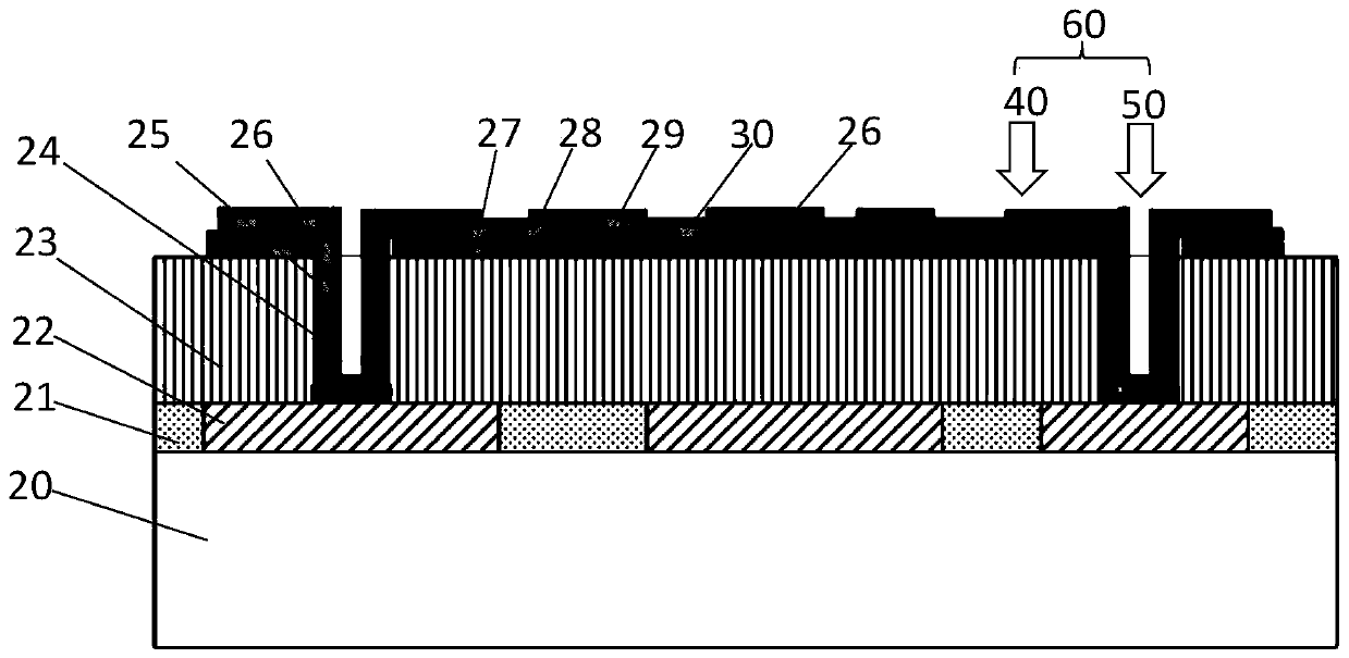
[0039] In the following specific embodiments of the present invention, please refer to figure 2 , figure 2 It is a structural schematic diagram of an infrared detector with a high filling factor according to a preferred embodiment of the present invention. Such as figure 2 As shown, an infrared detector structure with a high filling factor of t...


PUM


Abstract

The invention discloses an infrared detector structure with a high filling factor. The structure comprises a micro-bridge structure arranged on a substrate, and the micro-bridge structure comprises amicro-bridge floor, a support and an electric connection hole. The micro-bridge floor is sequentially provided with a first release protection layer, an infrared sensitive layer, a first metal electrode layer and a second release protection layer from bottom to top; a second metal electrode layer and a third release protection layer are sequentially arranged on the surface of the inner walls of the support and the electric connection hole; the second metal electrode layer is led out from an opening at the top of the inner walls of the support and electric connection hole, and is electrically connected with the first metal electrode layer; the second metal electrode layer achieves the electrical connection with the substrate through the support and the bottom opening of the electric connection hole, and the third release protection layer is led out from the support and the upper end opening part of the inner wall of the electric connection hole and is connected with the second release protection layer. The structure can further improve the product performance while improving the filling factor. The invention further discloses a manufacturing method of the infrared detector structurewith the high filling factor.

Description

technical field [0001] The present invention relates to the technical field of infrared detectors, in particular to an infrared detector structure with a high filling factor and a manufacturing method thereof. Background technique [0002] As infrared detector arrays get larger and larger, the area of ​​a single pixel is also shrinking. [0003] In the microbridge structure of the entire infrared pixel of the existing infrared detector, structures such as support holes and electrical connection holes are usually on the same layer as the bridge deck of the microbridge; and the support holes and electrical connection holes are photoetched in two steps process achieved. [0004] Please refer to figure 1 , figure 1 It is a structural schematic diagram of an existing infrared detector. Such as figure 1 As shown, the manufacturing steps of the infrared detector structure generally include: [0005] 1) depositing a sacrificial layer 11 on the substrate 10; [0006] 2) Patter...

Claims


Application Information

Patent Timeline
IPC IPC(8): H01L31/101H01L31/02
CPCH01L31/02002H01L31/101
Inventor 康晓旭
Owner SHANGHAI INTEGRATED CIRCUIT RES & DEV CENT
Learn More