

Bonding equipment and bonding method
A bonding and equipment technology, applied in semiconductor/solid-state device testing/measurement, semiconductor devices, electrical components, etc., can solve problems such as complex structure, low yield, and inconvenient electrical wiring of visual systems
- Summary
- Abstract
- Description
- Claims
- Application Information
AI Technical Summary
Problems solved by technology
Method used
Image

Examples
Embodiment 1
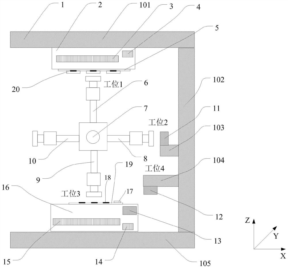
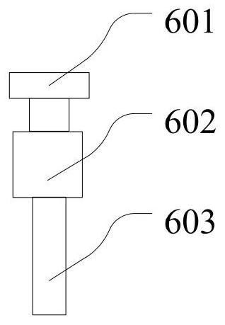
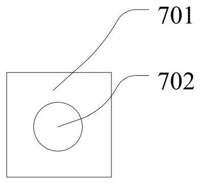
[0066] refer to figure 1 , which is a schematic structural diagram of the bonding equipment in Embodiment 1 of the present invention, the bonding equipment includes a supply motion table 2, a transmission system, a bonding motion table 16 and an alignment measurement system; the transmission system includes a rotation unit 7 and A plurality of chip bonding units uniformly arranged on the rotating unit 7, the rotating unit 7 drives the chip bonding unit to go back and forth between the chip picking station, the chip position measuring station and the chip bonding station in sequence The described supply motion table 2 carries some first chips, and the bonding motion table 16 carries some second chips; the chip bonding unit is used to pick up the first chip from the supply motion table 2, and The first chip is transferred and handed over to the corresponding second chip; and the alignment measurement system includes a first alignment measurement unit 11, a second alignment measu...
Embodiment 2
[0112] The chip alignment mark 18 is located on the side of the second chip facing away from the bonding motion table 16, and the chip identification mark can be located on the side of the first chip facing the supply motion table, or can also be located on the back side of the first chip. On the side facing the feeding motion table, when the chip identification mark is located on the side of the first chip facing away from the feeding motion table, the first alignment measurement unit 11 and the third alignment measurement unit 13 are the back side Align the measuring system. Specifically, see 14, Figure 14 It is a schematic structural diagram of the bonding equipment in Embodiment 2 of the present invention. Compared with Embodiment 1, the structural composition of the bonding equipment is different in that: the first alignment measurement unit 11 is a backside alignment measurement system, and its light source can be An infrared light source is used, which can penetrate t...
PUM
 Abstract
Description
Claims
Application Information